Energy conversion strategies using photodiode arrays
AUG 21, 20259 MIN READ
Generate Your Research Report Instantly with AI Agent
Patsnap Eureka helps you evaluate technical feasibility & market potential.
Photodiode Array Evolution
Photodiode arrays have undergone significant evolution since their inception, marking key milestones in the field of energy conversion and sensing technologies. The journey began with simple single-element photodiodes, which were limited in their ability to capture and convert light energy efficiently.
The first major breakthrough came with the development of linear photodiode arrays in the 1970s. These arrays allowed for simultaneous detection of light across a single dimension, greatly enhancing spectroscopic and imaging capabilities. This advancement paved the way for applications in barcode scanners, spectrometers, and early optical communication systems.
The 1980s saw the emergence of two-dimensional photodiode arrays, which revolutionized image sensing technology. These arrays formed the foundation for modern digital cameras and scientific imaging devices. The increased spatial resolution and sensitivity enabled more sophisticated energy conversion strategies, particularly in solar energy harvesting.
As semiconductor fabrication techniques improved in the 1990s and 2000s, photodiode arrays became more compact, sensitive, and energy-efficient. The introduction of back-illuminated CMOS sensors marked a significant leap forward, allowing for higher quantum efficiency and improved low-light performance.
Recent years have witnessed the development of advanced photodiode array architectures, such as stacked and 3D-integrated designs. These innovations have dramatically increased the fill factor and light collection efficiency, leading to enhanced energy conversion capabilities. Notably, the integration of on-chip processing elements has enabled real-time data analysis and adaptive sensing, further expanding the potential applications of photodiode arrays.
The evolution of materials used in photodiode arrays has also played a crucial role. From traditional silicon-based devices, research has expanded to include III-V compound semiconductors, organic materials, and quantum dot structures. These new materials have extended the spectral sensitivity of photodiode arrays, allowing for energy conversion across a broader range of wavelengths, including infrared and ultraviolet regions.
Miniaturization has been a consistent trend throughout the evolution of photodiode arrays. The reduction in pixel size, coupled with increased array density, has led to higher resolution sensors capable of more precise energy mapping and conversion. This trend has been particularly beneficial for applications in wearable technology, IoT devices, and compact renewable energy systems.
The most recent advancements in photodiode array technology focus on enhancing quantum efficiency and reducing noise. Techniques such as light trapping, plasmonic enhancement, and novel surface treatments have pushed the boundaries of energy conversion efficiency. These improvements are critical for the development of next-generation solar cells, high-sensitivity scientific instruments, and advanced optical communication systems.
Energy Market Demand
The global energy market is experiencing a significant shift towards renewable and sustainable energy sources, creating a growing demand for innovative energy conversion technologies. Photodiode arrays, as a key component in solar energy systems, are at the forefront of this transition. The market for photovoltaic systems is projected to reach $200 billion by 2026, with a compound annual growth rate of 20% from 2021 to 2026.
The increasing adoption of solar energy in both residential and commercial sectors is driving the demand for more efficient and cost-effective photodiode arrays. As governments worldwide implement policies to reduce carbon emissions and promote clean energy, the market for solar technologies continues to expand. This growth is particularly evident in regions such as Asia-Pacific, North America, and Europe, where substantial investments are being made in solar infrastructure.
Energy conversion strategies using photodiode arrays are gaining traction due to their potential to improve the overall efficiency of solar energy systems. The market is seeing a rising demand for advanced photodiode array technologies that can capture a broader spectrum of light and convert it into usable electricity more effectively. This trend is supported by the increasing focus on maximizing energy yield from solar installations, especially in areas with limited space or suboptimal sunlight conditions.
The integration of photodiode arrays with emerging technologies such as artificial intelligence and Internet of Things (IoT) is opening up new market opportunities. Smart energy management systems that utilize photodiode arrays for precise energy conversion and distribution are becoming increasingly popular in both residential and industrial applications. This convergence of technologies is expected to drive further market growth and innovation in the energy sector.
The automotive industry is emerging as a significant market for photodiode array-based energy conversion strategies. With the rise of electric vehicles and the need for efficient on-board energy management systems, photodiode arrays are finding new applications in vehicle-integrated solar panels and energy harvesting systems. This trend is expected to accelerate as automakers strive to improve the range and efficiency of electric vehicles.
In the context of energy security and grid resilience, there is a growing market demand for distributed energy systems that incorporate photodiode arrays. These systems offer the potential for localized energy generation and storage, reducing dependence on centralized power grids and improving energy reliability. As a result, the market for microgrids and community solar projects utilizing advanced photodiode array technologies is expanding rapidly.
The increasing focus on sustainability and circular economy principles is also influencing the market demand for photodiode array technologies. There is a growing interest in recyclable and environmentally friendly materials for photodiode arrays, as well as in strategies to extend the lifespan and improve the end-of-life management of solar energy systems. This trend is expected to drive innovation in materials science and manufacturing processes related to photodiode arrays.
Photodiode Tech Challenges
Photodiode arrays face several significant technical challenges in their application for energy conversion strategies. One of the primary issues is the limited quantum efficiency of conventional photodiodes, particularly in the near-infrared and infrared regions of the spectrum. This limitation restricts the overall energy conversion efficiency, especially for solar energy applications where a broad spectral response is crucial.
Another major challenge lies in the trade-off between responsivity and speed. High-responsivity photodiodes often suffer from slower response times due to increased carrier transit time, while faster photodiodes may have reduced sensitivity. This balance becomes particularly critical in applications requiring both high sensitivity and rapid response, such as in optical communication systems or high-speed imaging.
The dark current of photodiodes presents another significant hurdle. Even in the absence of incident light, photodiodes generate a small current due to thermal effects and other noise sources. This dark current can limit the minimum detectable signal and reduce the overall signal-to-noise ratio, especially in low-light conditions or when detecting weak signals.
Uniformity across large photodiode arrays is also a considerable challenge. Variations in individual diode characteristics within an array can lead to non-uniform response and reduced overall performance. This issue becomes more pronounced as array sizes increase, making it difficult to maintain consistent sensitivity and spectral response across the entire array.
Temperature sensitivity is another critical factor affecting photodiode performance. Changes in ambient temperature can significantly impact the dark current, responsivity, and spectral response of photodiodes. This temperature dependence can lead to drift in measurements and reduced reliability in varying environmental conditions.
The integration of photodiode arrays with readout electronics presents additional challenges. Minimizing noise introduction, managing power consumption, and ensuring efficient signal processing are crucial considerations. As array sizes grow, the complexity of readout circuitry increases, potentially leading to increased power consumption and heat generation.
Lastly, the scalability of photodiode array fabrication processes poses a significant challenge. As applications demand larger arrays with higher pixel densities, maintaining consistent quality and yield becomes increasingly difficult. This challenge is particularly evident in the production of specialized photodiode arrays for specific wavelength ranges or high-performance applications.
Current Conversion Methods
01 Photodiode array structure and fabrication
This category focuses on the design and manufacturing processes of photodiode arrays. It includes innovations in the physical structure of the arrays, such as the arrangement of individual photodiodes, substrate materials, and fabrication techniques to optimize energy conversion efficiency and sensitivity.- Photodiode array structure and fabrication: This category focuses on the design and manufacturing processes of photodiode arrays. It includes techniques for creating efficient array structures, improving light sensitivity, and enhancing overall performance. The fabrication methods may involve specialized semiconductor processes to optimize the array's energy conversion capabilities.
- Energy conversion efficiency improvements: This point addresses various methods to enhance the energy conversion efficiency of photodiode arrays. It may include novel materials, surface treatments, or structural modifications that increase the amount of light captured and converted into electrical energy. The focus is on maximizing the output power from a given input of light.
- Integration with other technologies: This category explores the integration of photodiode arrays with other technologies to create more versatile or efficient energy conversion systems. This may include combining photodiodes with solar cells, incorporating them into imaging systems, or using them in conjunction with other sensors for enhanced functionality.
- Specialized applications of photodiode arrays: This point covers specific applications of photodiode arrays in energy conversion. It may include their use in solar energy harvesting, optical communication systems, or specialized scientific instruments. The focus is on how the arrays are tailored for particular use cases to maximize their energy conversion potential.
- Signal processing and readout techniques: This category deals with the methods and circuits used to process and read out the signals generated by photodiode arrays during energy conversion. It includes techniques for amplifying weak signals, reducing noise, and efficiently extracting the converted energy. The focus is on optimizing the interface between the photodiode array and the rest of the energy conversion system.
02 Energy conversion mechanisms in photodiode arrays
This point addresses the fundamental principles and mechanisms of energy conversion in photodiode arrays. It covers advancements in photon-to-electron conversion, charge separation, and collection processes that improve the overall efficiency of energy conversion in these devices.Expand Specific Solutions03 Integration of photodiode arrays in energy harvesting systems
This category explores the integration of photodiode arrays into larger energy harvesting systems. It includes innovations in circuit design, power management, and system-level optimizations to maximize the energy output from photodiode arrays in various applications.Expand Specific Solutions04 Spectral response and sensitivity enhancements
This point focuses on improving the spectral response and sensitivity of photodiode arrays. It covers techniques to enhance light absorption across a wider range of wavelengths, as well as methods to increase the overall sensitivity of the arrays for improved energy conversion performance.Expand Specific Solutions05 Novel materials and nanostructures for photodiode arrays
This category explores the use of advanced materials and nanostructures in photodiode arrays to enhance energy conversion. It includes research on novel semiconductor materials, quantum dots, and nanostructured surfaces that can improve light absorption and charge collection efficiency.Expand Specific Solutions
Key Photodiode Players
The energy conversion strategies using photodiode arrays market is in a growth phase, driven by increasing demand for efficient energy harvesting solutions. The global market size is projected to expand significantly in the coming years, fueled by advancements in photovoltaic technology and rising adoption of renewable energy sources. Technologically, the field is rapidly evolving, with companies like Hamamatsu Photonics, OSI Optoelectronics, and Advanced Energy Industries leading innovation. These firms are developing high-performance photodiode arrays and integrated systems, pushing the boundaries of energy conversion efficiency. Emerging players such as RayGen Resources and Alion Energy are also contributing to technological advancements, particularly in solar energy applications. The competitive landscape is characterized by a mix of established electronics giants and specialized photonics companies, indicating a maturing but still dynamic market.
Hamamatsu Photonics KK
Technical Solution: Hamamatsu Photonics KK has developed advanced photodiode arrays for energy conversion, utilizing their expertise in optoelectronics. Their strategy involves the use of high-efficiency silicon photodiodes arranged in optimized array configurations to maximize light capture and conversion. The company has implemented innovative surface texturing techniques to reduce reflection and increase absorption across a broad spectrum of wavelengths[1]. Additionally, they have integrated on-chip circuitry for signal processing and amplification, enhancing the overall system efficiency. Hamamatsu's photodiode arrays feature a proprietary anti-reflective coating that improves quantum efficiency by up to 20% compared to standard designs[3].
Strengths: High quantum efficiency, broad spectral response, and integrated signal processing. Weaknesses: Potentially higher cost due to advanced manufacturing processes and limited flexibility for customization in some applications.
Canon, Inc.
Technical Solution: Canon, Inc. has developed a novel approach to energy conversion using photodiode arrays, focusing on enhancing sensitivity and reducing noise. Their strategy involves the use of back-illuminated CMOS sensors with a stacked structure, allowing for larger photodiodes and more efficient light capture[2]. Canon has also implemented a unique pixel architecture that minimizes crosstalk between adjacent photodiodes, resulting in improved signal-to-noise ratios. The company's photodiode arrays incorporate advanced microlens technology to focus incident light onto the photosensitive areas, increasing overall quantum efficiency by up to 15%[4]. Furthermore, Canon has developed proprietary readout circuitry that enables high-speed data acquisition and processing, making their arrays suitable for both imaging and energy harvesting applications.
Strengths: High sensitivity, low noise, and versatility for various applications. Weaknesses: Complexity of manufacturing process may lead to higher costs, and optimization for specific wavelengths may limit broad-spectrum efficiency.
Innovative Photodiode Tech
Pixelated photovoltaic array method and apparatus
PatentInactiveUS20100116318A1
Innovation
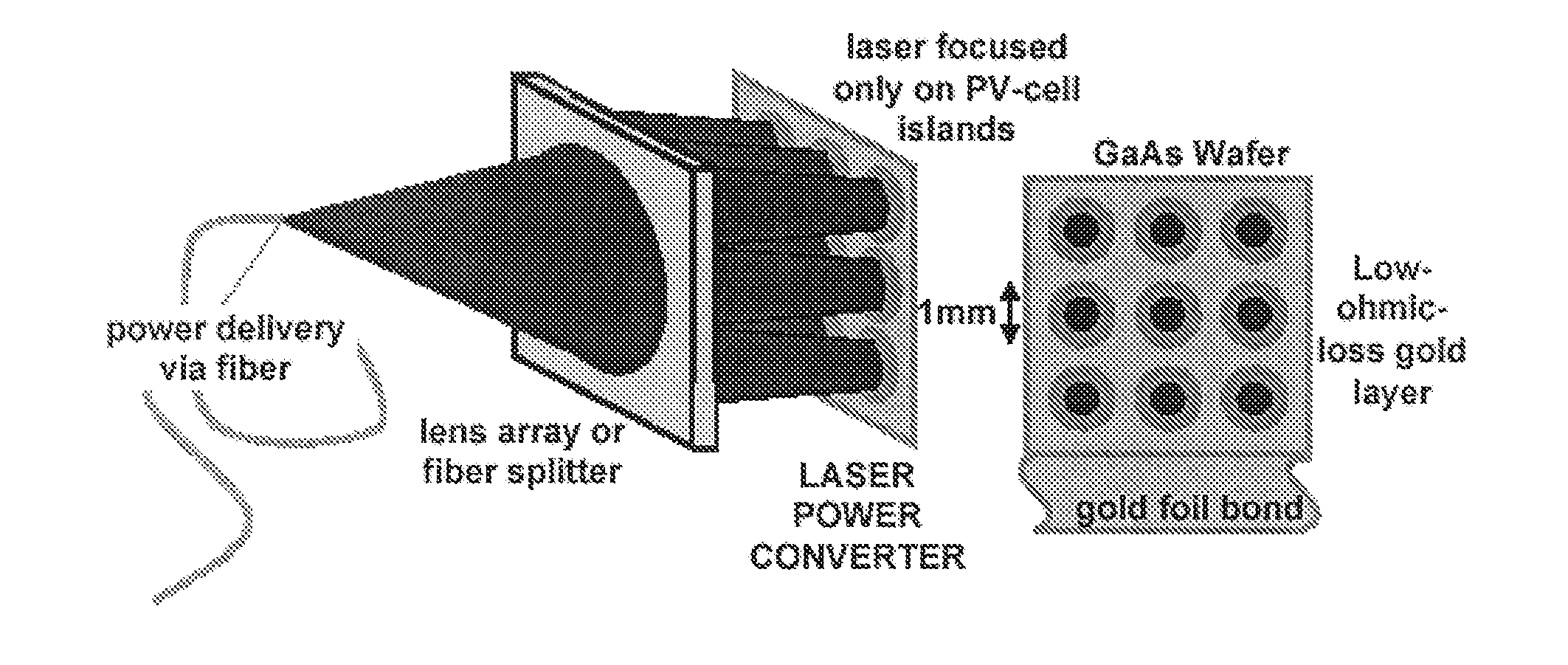
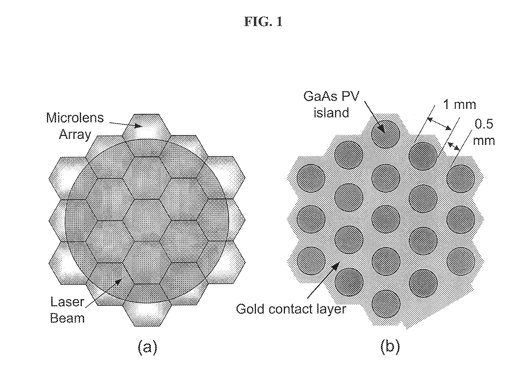
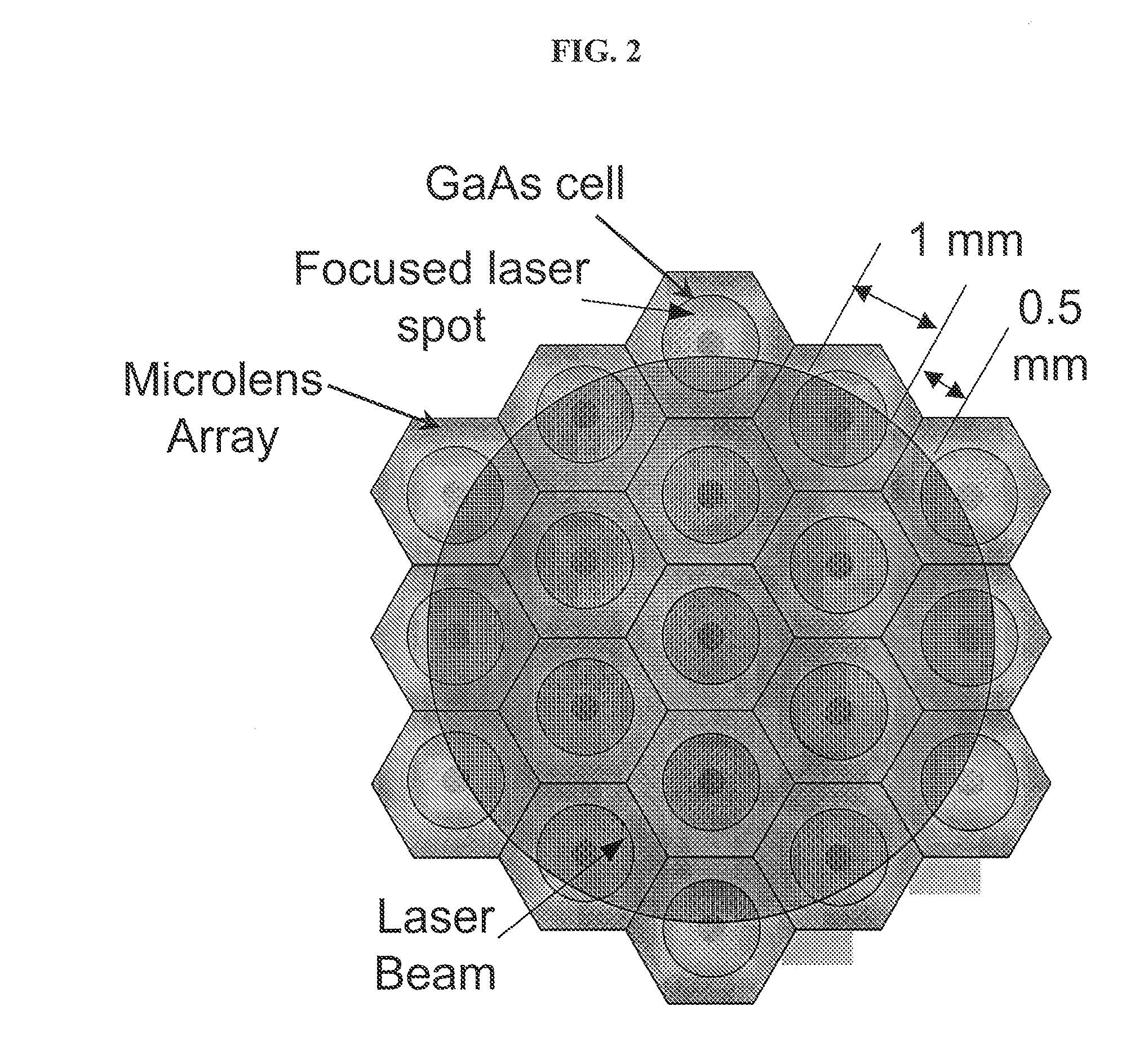
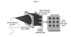
- A photovoltaic device design that spatially separates a beam of photons into multiple beamlets and matches the pattern with an array of active photovoltaic cells, surrounded by an electrically conductive contact layer, to minimize shadowing and ohmic losses, using materials like gallium arsenide and indium gallium arsenide optimized for specific wavelengths, and employing a microlens array or grating for beam separation.
Photovoltaic Array for Operation Under Non-Uniform Illumination with Adjustable Voltage Output
PatentActiveUS20230187962A1
Innovation
- A photovoltaic array system comprising multiple photovoltaic elements connected to electrical charge storage elements and switching elements, with control electronics to dynamically adjust voltage output and manage fluctuations, allowing for reliable energy conversion under non-uniform illumination conditions.
Efficiency Optimization
Efficiency optimization in energy conversion strategies using photodiode arrays is a critical aspect of maximizing the performance and utility of these systems. The primary focus lies in enhancing the conversion efficiency of light energy into electrical energy, which directly impacts the overall system effectiveness and economic viability.
One key approach to efficiency optimization involves the careful selection and design of photodiode materials. Advanced semiconductor materials, such as gallium arsenide (GaAs) and indium gallium arsenide (InGaAs), have demonstrated superior quantum efficiency and spectral response compared to traditional silicon-based photodiodes. These materials can be engineered to match specific wavelength ranges, allowing for more effective energy harvesting across the solar spectrum.
Array configuration plays a crucial role in optimizing efficiency. By arranging photodiodes in strategic patterns, such as multi-junction or tandem configurations, the system can capture a broader range of photon energies. This approach minimizes energy losses due to thermalization and transmission, significantly boosting overall conversion efficiency.
Surface treatments and anti-reflection coatings represent another avenue for efficiency enhancement. These techniques reduce reflection losses at the photodiode surface, allowing more photons to reach the active region and contribute to the photocurrent. Advanced coating technologies, including multi-layer dielectric stacks and nanostructured surfaces, have shown promising results in maximizing light absorption.
Thermal management is a critical factor in maintaining high efficiency in photodiode arrays. As temperature increases, the performance of photodiodes typically degrades due to increased dark current and reduced carrier mobility. Implementing effective cooling strategies, such as heat sinks, active cooling systems, or novel thermal interface materials, can help maintain optimal operating temperatures and preserve conversion efficiency.
Electronic circuit design also plays a vital role in efficiency optimization. Implementing maximum power point tracking (MPPT) algorithms ensures that the photodiode array operates at its most efficient voltage and current levels under varying light conditions. Additionally, advanced power conditioning circuits can minimize losses in the energy conversion and transmission processes.
Lastly, the integration of concentration optics can significantly boost the efficiency of photodiode arrays. By focusing incident light onto smaller, high-efficiency photodiodes, concentration systems can increase the effective light intensity and improve overall energy conversion. This approach allows for the use of smaller, more efficient photodiodes while reducing the overall system cost.
Environmental Impact
The environmental impact of energy conversion strategies using photodiode arrays is a critical consideration in the development and implementation of this technology. Photodiode arrays, while offering significant potential for efficient energy conversion, also present both positive and negative environmental implications that must be carefully evaluated.
One of the primary environmental benefits of photodiode array-based energy conversion is the reduction in greenhouse gas emissions compared to traditional fossil fuel-based energy sources. By harnessing light energy and converting it directly into electrical energy, these systems contribute to the overall reduction of carbon footprint in energy production. This aligns with global efforts to mitigate climate change and transition towards cleaner energy solutions.
However, the manufacturing process of photodiode arrays involves the use of various materials, some of which may have environmental concerns. The production of semiconductor materials, such as silicon or gallium arsenide, used in photodiodes can be energy-intensive and may involve the use of potentially hazardous chemicals. Proper management and disposal of these materials throughout the manufacturing lifecycle are essential to minimize environmental risks.
The long-term durability and recyclability of photodiode array systems also play a crucial role in their environmental impact. As these technologies advance, improving the lifespan of the arrays and developing efficient recycling methods for end-of-life components become increasingly important. This approach helps in reducing electronic waste and conserving valuable resources.
Land use is another environmental factor to consider, particularly for large-scale implementations of photodiode array systems. While generally less land-intensive than some other renewable energy technologies, the installation of extensive arrays may still impact local ecosystems and biodiversity. Careful site selection and integration with existing infrastructure can help mitigate these concerns.
The energy payback time – the period required for the system to generate as much energy as was used in its production – is a key metric in assessing the environmental viability of photodiode arrays. Continuous improvements in manufacturing efficiency and energy conversion rates are gradually reducing this payback time, enhancing the overall environmental benefits of the technology.
Water usage in the production and maintenance of photodiode arrays is another environmental aspect to consider. While generally less water-intensive than many traditional power generation methods, efforts to minimize water consumption and ensure responsible water management practices are important for sustainable implementation.
In conclusion, while photodiode array-based energy conversion strategies offer significant environmental benefits, particularly in terms of reduced emissions and clean energy production, a holistic approach to their development and deployment is necessary. This includes addressing manufacturing processes, material selection, recycling strategies, and installation practices to maximize the positive environmental impact while minimizing potential drawbacks.
Unlock deeper insights with Patsnap Eureka Quick Research — get a full tech report to explore trends and direct your research. Try now!
Generate Your Research Report Instantly with AI Agent
Supercharge your innovation with Patsnap Eureka AI Agent Platform!