How photodiodes enhance digital image quality in cameras
AUG 21, 20259 MIN READ
Generate Your Research Report Instantly with AI Agent
Patsnap Eureka helps you evaluate technical feasibility & market potential.
Photodiode Technology Evolution and Objectives
Photodiodes have played a pivotal role in the evolution of digital imaging technology, revolutionizing the way cameras capture and process light. The journey of photodiode technology in digital cameras began in the late 20th century, with significant advancements occurring over the past few decades.
Initially, charge-coupled devices (CCDs) dominated the digital camera market. These sensors utilized photodiodes to convert light into electrical charges, which were then transferred and read out sequentially. While CCDs offered high image quality, they were power-hungry and relatively slow in processing speeds.
The advent of complementary metal-oxide-semiconductor (CMOS) image sensors marked a significant milestone in photodiode technology. CMOS sensors integrated photodiodes with amplification and digitization circuitry on a single chip, offering advantages in power efficiency, speed, and cost-effectiveness. This breakthrough led to the widespread adoption of CMOS sensors in digital cameras, smartphones, and other imaging devices.
As technology progressed, manufacturers focused on enhancing the light sensitivity and dynamic range of photodiodes. Back-illuminated sensor designs emerged, allowing more light to reach the photodiodes by placing the metal wiring behind the light-sensitive layer. This innovation significantly improved low-light performance and overall image quality.
The pursuit of higher resolution and better color accuracy drove the development of smaller, more efficient photodiodes. Pixel binning techniques were introduced to balance resolution and light sensitivity, particularly in challenging lighting conditions. Additionally, advancements in microlens technology helped funnel more light onto each photodiode, further improving light-gathering capabilities.
Recent years have seen the emergence of stacked CMOS sensors, where the photodiode layer is separated from the processing circuitry. This architecture allows for larger photodiodes and more sophisticated on-chip processing, resulting in superior image quality and faster readout speeds.
Looking ahead, the objectives for photodiode technology in digital cameras are multifaceted. Researchers aim to further improve light sensitivity, expand dynamic range, and reduce noise levels to enhance image quality across various lighting conditions. There is also a focus on developing photodiodes with broader spectral sensitivity, potentially enabling cameras to capture information beyond the visible spectrum.
Another key goal is to increase the speed and efficiency of photodiodes, enabling higher frame rates for video capture and faster autofocus systems. Additionally, efforts are underway to integrate advanced computational photography techniques directly into the sensor, leveraging the capabilities of photodiodes to capture more detailed scene information for post-processing.
Digital Camera Market Trends
The digital camera market has undergone significant transformations in recent years, driven by technological advancements and changing consumer preferences. Smartphone cameras have become increasingly sophisticated, posing a challenge to traditional digital camera manufacturers. However, this has also spurred innovation in the dedicated camera segment, with a focus on high-end models and specialized features.
The global digital camera market size was valued at approximately $24.3 billion in 2020 and is projected to reach $32.1 billion by 2027, growing at a CAGR of 3.8% during the forecast period. This growth is primarily attributed to the increasing demand for high-quality imaging devices in various sectors, including professional photography, filmmaking, and surveillance.
One of the key trends in the digital camera market is the shift towards mirrorless cameras. These devices offer advantages such as compact size, lighter weight, and improved autofocus capabilities compared to traditional DSLRs. Major camera manufacturers like Canon, Nikon, and Sony have invested heavily in developing their mirrorless product lines, catering to both professional and enthusiast photographers.
Another significant trend is the integration of advanced technologies like artificial intelligence (AI) and machine learning into digital cameras. These technologies enhance image processing capabilities, improve autofocus performance, and enable features such as intelligent scene recognition and automatic image optimization. This trend aligns with the growing demand for cameras that can produce high-quality images with minimal user intervention.
The rise of content creation for social media platforms has also influenced the digital camera market. There is an increasing demand for cameras with features tailored for vlogging and live streaming, such as flip-out screens, built-in Wi-Fi connectivity, and improved video capabilities. This has led to the development of hybrid cameras that excel in both still photography and video recording.
In terms of image sensors, there is a continued push towards higher resolutions and improved low-light performance. Full-frame sensors are becoming more prevalent in mid-range cameras, while medium format sensors are gaining traction in the high-end professional segment. Additionally, advancements in sensor technology, including the development of stacked CMOS sensors, are contributing to enhanced image quality and faster readout speeds.
The market is also witnessing a growing emphasis on rugged and weather-sealed cameras, catering to outdoor enthusiasts and professionals working in challenging environments. This trend is particularly evident in the action camera segment, where manufacturers are focusing on durability, waterproofing, and advanced stabilization technologies.
Photodiode Integration Challenges
The integration of photodiodes into digital cameras presents several significant challenges that manufacturers and engineers must overcome to enhance image quality effectively. One of the primary obstacles is the miniaturization of photodiode arrays while maintaining or improving their light-sensing capabilities. As camera sensors become smaller, particularly in mobile devices, fitting a sufficient number of photodiodes into a compact space without compromising their performance becomes increasingly difficult.
Another critical challenge lies in managing the trade-off between pixel size and light sensitivity. Smaller pixels allow for higher resolution images but typically capture less light, potentially leading to increased noise in low-light conditions. Conversely, larger pixels offer better light sensitivity but limit the overall resolution of the sensor. Striking the right balance between these factors is crucial for optimal image quality across various lighting scenarios.
The issue of cross-talk between adjacent photodiodes also poses a significant integration challenge. As pixel density increases, the risk of light from one pixel bleeding into neighboring pixels grows, potentially causing color inaccuracies and reduced sharpness. Implementing effective isolation techniques between photodiodes is essential to maintain image integrity and color fidelity.
Heat management is another critical concern in photodiode integration. As camera sensors become more powerful and compact, the heat generated during operation can affect the performance of photodiodes, potentially leading to increased noise and reduced image quality. Developing efficient heat dissipation mechanisms within the limited space of modern camera modules is a complex engineering challenge.
Furthermore, the integration of advanced features such as phase detection autofocus (PDAF) or dual-pixel autofocus systems introduces additional complexities. These technologies require specialized photodiode designs and arrangements, which must be seamlessly integrated without compromising the overall image quality or increasing the sensor size significantly.
The manufacturing process itself presents challenges in terms of yield and consistency. Producing high-quality photodiode arrays at scale, with uniform performance across all pixels, requires precise fabrication techniques and stringent quality control measures. Any defects or variations in the manufacturing process can lead to inconsistencies in image quality across different camera units.
Lastly, the integration of photodiodes must also consider the broader ecosystem of camera components, including lenses, image processors, and software algorithms. Ensuring optimal compatibility and synergy between these elements is crucial for maximizing the benefits of advanced photodiode technology in enhancing digital image quality.
Current Photodiode Implementation Strategies
01 Pixel structure optimization
Improving the pixel structure of photodiodes can enhance image quality. This includes optimizing the size, shape, and arrangement of pixels to increase light sensitivity and reduce noise. Advanced pixel designs can incorporate light guides, microlenses, or other optical elements to improve light collection efficiency and overall image quality.- Pixel structure optimization: Improving the pixel structure of photodiodes can enhance image quality. This includes optimizing the size, shape, and arrangement of pixels to increase light sensitivity and reduce noise. Advanced pixel designs can also incorporate light guides or microlenses to improve light collection efficiency.
- Color filter array improvements: Enhancing color filter arrays used in conjunction with photodiodes can lead to better color reproduction and overall image quality. This involves developing new color filter materials, optimizing their spectral characteristics, and improving their arrangement to capture more accurate color information.
- Noise reduction techniques: Implementing various noise reduction techniques can significantly improve image quality in photodiode-based sensors. This includes developing advanced readout circuits, implementing correlated double sampling, and utilizing on-chip noise cancellation algorithms to minimize dark current and other sources of noise.
- High dynamic range imaging: Incorporating high dynamic range (HDR) capabilities in photodiode-based image sensors can greatly enhance image quality, especially in challenging lighting conditions. This involves developing specialized pixel architectures, implementing multiple exposure techniques, and utilizing advanced signal processing algorithms to capture a wider range of light intensities.
- Back-illuminated sensor design: Utilizing back-illuminated sensor designs can improve the light sensitivity and overall performance of photodiode-based image sensors. This approach involves placing the photodiode layer closer to the light source, reducing light loss and improving quantum efficiency, resulting in better image quality, especially in low-light conditions.
02 Color filter array improvements
Enhancing color filter arrays used in conjunction with photodiodes can significantly improve image quality. This involves developing new color filter materials, optimizing filter patterns, and implementing advanced color separation techniques to achieve better color accuracy and resolution in captured images.Expand Specific Solutions03 Noise reduction techniques
Implementing various noise reduction techniques can greatly improve image quality in photodiode-based imaging systems. This includes developing advanced readout circuits, implementing correlated double sampling, and utilizing on-chip noise cancellation algorithms to minimize dark current, reset noise, and other sources of image degradation.Expand Specific Solutions04 High dynamic range imaging
Incorporating high dynamic range (HDR) imaging techniques can significantly enhance image quality, especially in challenging lighting conditions. This involves developing specialized photodiode structures, implementing multiple exposure techniques, or utilizing advanced signal processing algorithms to capture and process a wider range of light intensities.Expand Specific Solutions05 3D integration and stacked sensor designs
Utilizing 3D integration techniques and stacked sensor designs can improve image quality by allowing for more sophisticated photodiode structures and increased functionality. This approach enables the integration of advanced processing capabilities, larger pixel areas, and improved light collection efficiency, resulting in enhanced overall image quality.Expand Specific Solutions
Key Players in Photodiode Manufacturing
The photodiode technology for enhancing digital image quality in cameras is in a mature stage of development, with a substantial market size driven by the widespread adoption of digital imaging devices. The technology's maturity is evident from the involvement of major players like Sony Semiconductor Solutions, Samsung Electronics, and OmniVision Technologies, who have established strong positions in the market. These companies, along with others like Canon and FUJIFILM, are continuously innovating to improve sensor performance, focusing on aspects such as low-light sensitivity, dynamic range, and resolution. The competitive landscape is characterized by intense research and development efforts, with companies like Micron Technology and Taiwan Semiconductor Manufacturing Co. contributing to advancements in sensor fabrication processes.
Sony Semiconductor Solutions Corp.
Technical Solution: Sony Semiconductor Solutions Corp. has developed advanced photodiode technology for enhancing digital image quality in cameras. Their Exmor RS CMOS image sensor utilizes a stacked structure with back-illuminated pixel array and separate signal processing circuits[1]. This design allows for larger photodiodes, increasing light sensitivity and reducing noise. The company has also implemented copper wiring in their sensors, which improves readout speeds and enables high-speed image capturing[2]. Additionally, Sony has developed intelligent noise reduction algorithms that work in conjunction with their photodiodes to further improve image quality in low-light conditions[3].
Strengths: Superior light sensitivity, reduced noise, and high-speed image capture. Weaknesses: Potentially higher production costs and complexity in manufacturing process.
Samsung Electronics Co., Ltd.
Technical Solution: Samsung Electronics has developed ISOCELL technology for their image sensors, which enhances photodiode performance and improves digital image quality. The ISOCELL structure reduces crosstalk between pixels by placing a physical barrier between neighboring pixels[4]. This allows each photodiode to capture more light, resulting in improved color accuracy and reduced noise. Samsung has also implemented Dual Pixel technology, where each pixel contains two photodiodes for faster and more accurate autofocus[5]. Furthermore, their latest sensors incorporate Tetracell technology, which combines four pixels into one larger pixel in low-light conditions, effectively increasing light sensitivity[6].
Strengths: Improved color accuracy, reduced noise, and enhanced low-light performance. Weaknesses: Potential loss of resolution in low-light conditions when using pixel-binning techniques.
Innovative Photodiode Designs for Cameras
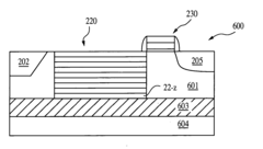
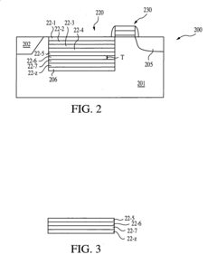
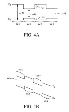
High gain, low noise photodiode for image sensors and method of formation
PatentInactiveUS20050040445A1
Innovation
- A pixel cell with a photodiode having a heterostructure composed of layers with different band gaps, promoting impact ionization by one type of charge carrier and suppressing it by the other, thereby reducing noise and dark current, and using materials like Si, SiGe, and Group III-V materials for charge amplification.
Photodiode assembly
PatentWO2022150126A1
Innovation
- A photodiode assembly with a controllable voltage biasing source and control inputs influences electron flow, utilizing reverse biasing to increase the depletion zone and multiplication effect, allowing electrons to flow through capacitors for accurate charge measurement, thereby enabling smaller pixels, reduced dark current, and improved low-light performance.
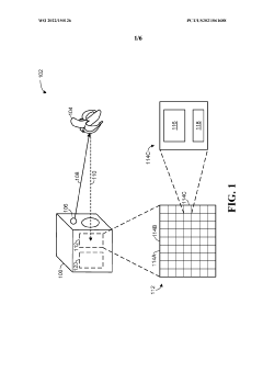
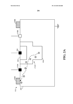
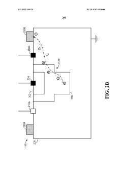
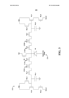
Image Quality Metrics and Standards
Image quality metrics and standards play a crucial role in evaluating and enhancing the performance of photodiodes in digital cameras. These metrics provide quantitative measures to assess various aspects of image quality, enabling manufacturers and researchers to optimize camera systems and improve overall image fidelity.
One of the primary metrics used in evaluating image quality is the Signal-to-Noise Ratio (SNR). This measure compares the level of desired signal to the level of background noise, with higher SNR values indicating better image quality. Photodiodes contribute significantly to improving SNR by efficiently converting light into electrical signals, minimizing noise introduction during the conversion process.
Another important metric is the Dynamic Range (DR), which represents the camera's ability to capture both very bright and very dark areas within a single image. Photodiodes with high sensitivity and low noise characteristics help extend the dynamic range, allowing for more detailed and balanced images across varying lighting conditions.
Resolution is a fundamental aspect of image quality, often measured in terms of Modulation Transfer Function (MTF). MTF quantifies the camera's ability to reproduce fine details and sharp edges. Advanced photodiode designs with improved quantum efficiency and reduced crosstalk between pixels contribute to higher MTF values, resulting in sharper and more detailed images.
Color accuracy is assessed using metrics such as Color Reproduction Error and Color Gamut Coverage. Photodiodes with enhanced spectral response and color filter arrays help achieve more accurate color reproduction, expanding the range of capturable colors and improving overall color fidelity.
The ISO standard 12233 provides guidelines for measuring the resolution of digital cameras, while ISO 15739 focuses on noise measurements. These standards ensure consistency in evaluating and comparing different camera systems. Manufacturers often use these standards to optimize their photodiode designs and signal processing algorithms.
Image quality standards also address factors like lens distortion, chromatic aberration, and vignetting. While these are primarily optical issues, advanced photodiode arrays and image processing techniques can help mitigate their effects, contributing to overall image quality improvement.
As technology advances, new metrics and standards continue to emerge. For instance, the development of high dynamic range (HDR) imaging has led to the introduction of specific HDR quality metrics. Similarly, the increasing prevalence of computational photography techniques has sparked discussions on new standards to evaluate the performance of AI-enhanced imaging systems.
Environmental Impact of Photodiode Production
The production of photodiodes, essential components in digital cameras for enhancing image quality, has significant environmental implications. The manufacturing process involves several stages, each with its own ecological footprint.
Raw material extraction is the first step, requiring mining operations for silicon and other semiconductor materials. These activities can lead to habitat destruction, soil erosion, and water pollution. The refining of these materials often involves energy-intensive processes and the use of hazardous chemicals, contributing to air and water pollution.
The fabrication of photodiodes takes place in cleanroom environments, which demand substantial energy for maintaining precise temperature and humidity levels. This constant climate control results in high electricity consumption and associated carbon emissions. Additionally, the production process utilizes various chemicals, including dopants and etching agents, which can be harmful if not properly managed.
Water usage is another critical environmental concern in photodiode production. The manufacturing process requires large volumes of ultra-pure water for cleaning and processing, potentially straining local water resources. The resulting wastewater often contains trace amounts of chemicals and metals, necessitating extensive treatment before release.
Electronic waste (e-waste) is a growing issue as digital cameras and other devices containing photodiodes reach end-of-life. Improper disposal can lead to the leaching of toxic substances into soil and groundwater. Recycling efforts are crucial but face challenges due to the complex nature of electronic components.
The global supply chain for photodiode production also contributes to its environmental impact. Transportation of raw materials, components, and finished products across long distances increases carbon emissions. Furthermore, the demand for rare earth elements in some advanced photodiode designs can drive environmentally damaging mining practices in certain regions.
However, it's important to note that the environmental impact of photodiode production should be considered in the context of their benefits. By enhancing digital image quality, photodiodes contribute to the efficiency and longevity of cameras, potentially reducing the need for frequent device replacements and thus mitigating overall electronic waste.
Efforts to improve the sustainability of photodiode production are ongoing. These include developing more energy-efficient manufacturing processes, implementing closed-loop water systems, and exploring alternative materials with lower environmental impacts. Additionally, advancements in recycling technologies are helping to recover valuable materials from discarded electronics, reducing the demand for new raw material extraction.
Unlock deeper insights with Patsnap Eureka Quick Research — get a full tech report to explore trends and direct your research. Try now!
Generate Your Research Report Instantly with AI Agent
Supercharge your innovation with Patsnap Eureka AI Agent Platform!