Photodiode criteria for high-precision laboratory instruments
AUG 21, 20259 MIN READ
Generate Your Research Report Instantly with AI Agent
Patsnap Eureka helps you evaluate technical feasibility & market potential.
Photodiode Tech Evolution
The evolution of photodiodes for high-precision laboratory instruments has been marked by significant advancements in materials science, manufacturing processes, and device design. In the early stages, silicon-based photodiodes dominated the market, offering reasonable sensitivity and reliability. However, as the demands for higher precision and broader spectral response grew, new materials and structures emerged.
The 1970s and 1980s saw the introduction of PIN (Positive-Intrinsic-Negative) photodiodes, which offered improved sensitivity and faster response times compared to their predecessors. This development was crucial for applications requiring rapid light detection and measurement in laboratory settings. Concurrently, avalanche photodiodes (APDs) were developed, providing internal gain mechanisms that significantly enhanced sensitivity for low-light applications.
The 1990s brought about the widespread adoption of indium gallium arsenide (InGaAs) photodiodes, particularly for near-infrared applications. These devices extended the spectral range beyond silicon's capabilities, enabling more diverse and specialized laboratory instruments. During this period, improvements in manufacturing techniques also led to the production of larger area photodiodes with enhanced uniformity and lower noise characteristics.
The turn of the millennium saw a focus on enhancing quantum efficiency and reducing dark current in photodiodes. Novel surface treatments and passivation techniques were developed to minimize surface recombination and improve overall performance. Additionally, the integration of photodiodes with on-chip amplifiers and readout circuits became more common, leading to the development of highly sensitive and compact photodetector modules.
In recent years, the push for even higher precision has driven research into new materials and structures. Silicon carbide (SiC) photodiodes have gained attention for their ability to operate in harsh environments and their low dark current properties. Graphene-based photodetectors have also emerged as a promising technology, offering ultra-fast response times and broadband sensitivity.
The latest trends in photodiode technology for high-precision laboratory instruments include the development of multi-junction photodiodes for enhanced spectral response and the exploration of nanostructured materials to improve light absorption and carrier collection efficiency. Additionally, there is a growing interest in integrating artificial intelligence and machine learning algorithms with photodiode systems to enhance data processing and calibration capabilities.
As we look to the future, the evolution of photodiodes is likely to continue focusing on improving key performance metrics such as responsivity, noise equivalent power, and linearity across a wider range of operating conditions. The integration of advanced materials, novel device architectures, and sophisticated signal processing techniques will play a crucial role in meeting the ever-increasing demands of high-precision laboratory instrumentation.
Market Analysis
The market for high-precision photodiodes in laboratory instruments has been experiencing steady growth, driven by increasing demand for accurate and sensitive measurement devices across various scientific and industrial applications. This growth is particularly evident in fields such as spectroscopy, photometry, and optical communication, where precise light detection is crucial.
The global market for photodiodes in high-precision laboratory instruments is expected to continue its upward trajectory, with a compound annual growth rate (CAGR) projected to be in the mid-single digits over the next five years. This growth is attributed to the expanding research and development activities in both academic and industrial sectors, as well as the increasing adoption of advanced analytical techniques in fields like life sciences, material science, and environmental monitoring.
One of the key factors driving market demand is the continuous improvement in photodiode technology, leading to enhanced sensitivity, faster response times, and lower noise levels. These advancements are enabling researchers and scientists to achieve more accurate and reliable results in their experiments and analyses. Additionally, the integration of photodiodes with other technologies, such as microfluidics and nanotechnology, is opening up new application areas and further fueling market growth.
The market for high-precision photodiodes is also benefiting from the growing trend towards automation and digitalization in laboratories. As more laboratories adopt automated systems and robotics for their research processes, the need for high-performance photodiodes that can seamlessly integrate with these systems is increasing. This trend is particularly strong in pharmaceutical and biotechnology industries, where high-throughput screening and automated assays are becoming standard practice.
Geographically, North America and Europe currently dominate the market for high-precision photodiodes in laboratory instruments, owing to their well-established research infrastructure and significant investments in scientific research. However, the Asia-Pacific region is expected to witness the fastest growth in the coming years, driven by increasing research and development expenditure in countries like China, Japan, and South Korea.
The market landscape is characterized by a mix of large, established players and innovative start-ups. While established companies leverage their brand reputation and extensive distribution networks, start-ups are often at the forefront of technological innovation, introducing novel photodiode designs and materials. This competitive environment is fostering continuous innovation and driving down costs, making high-precision photodiodes more accessible to a wider range of laboratories and research institutions.
Despite the positive outlook, the market faces challenges such as the high cost of advanced photodiodes and the need for specialized knowledge to integrate and operate these devices effectively. However, ongoing research into new materials and manufacturing techniques is expected to address these challenges, potentially leading to more cost-effective and user-friendly solutions in the future.
Current Challenges
The development of high-precision laboratory instruments utilizing photodiodes faces several significant challenges in the current technological landscape. One of the primary obstacles is the inherent noise in photodiode sensors, which can significantly impact the accuracy and reliability of measurements. This noise, including shot noise, thermal noise, and 1/f noise, becomes particularly problematic when dealing with low-light conditions or attempting to detect minute changes in light intensity.
Another critical challenge lies in the temperature sensitivity of photodiodes. Fluctuations in ambient temperature can lead to variations in the photodiode's response, affecting the consistency and precision of measurements. This issue is especially pronounced in applications requiring long-term stability or those operating in environments with variable temperature conditions.
The limited dynamic range of photodiodes presents a further hurdle for high-precision instruments. Many advanced laboratory applications demand the ability to accurately measure both very low and very high light intensities, often within the same experiment. Achieving this wide dynamic range while maintaining high precision across the entire spectrum is a complex engineering challenge.
Linearity of response is another area of concern. While photodiodes generally exhibit good linearity, deviations can occur, especially at very low or very high light intensities. These non-linearities can introduce errors in measurements, particularly in applications requiring absolute accuracy across a wide range of light levels.
The speed of response and recovery time of photodiodes also pose challenges for certain high-precision applications. Some experiments require rapid detection of light intensity changes, and the inherent capacitance and charge carrier transit times in photodiodes can limit their ability to respond to fast optical signals.
Spectral response characteristics present another set of challenges. Different photodiode materials and designs have varying sensitivities across the light spectrum. Achieving uniform sensitivity across a broad range of wavelengths, or precisely tailoring the spectral response for specific applications, remains a significant technical hurdle.
Lastly, the integration of photodiodes into complex laboratory instruments introduces challenges related to signal processing and data acquisition. Extracting clean, accurate signals from photodiodes in the presence of various noise sources and potential interference requires sophisticated electronic design and signal processing techniques. This becomes even more critical as instruments push the boundaries of precision and sensitivity.
State-of-the-Art Solutions
01 Improved photodiode structure
Enhancing photodiode precision through structural improvements, such as optimized doping profiles, reduced dark current, and increased quantum efficiency. These advancements result in better signal-to-noise ratios and improved overall performance.- Structural design for improved precision: Enhancing photodiode precision through structural improvements, such as optimizing the layout of the photodiode and surrounding components. This includes techniques like reducing parasitic capacitance, implementing guard rings, and utilizing advanced packaging methods to minimize noise and increase sensitivity.
- Integration with readout circuits: Integrating photodiodes with specialized readout circuits to improve overall precision. This involves designing low-noise amplifiers, implementing correlated double sampling techniques, and utilizing advanced analog-to-digital converters to enhance signal processing and reduce noise in the output.
- Temperature compensation techniques: Implementing temperature compensation methods to maintain photodiode precision across varying environmental conditions. This includes using temperature sensors, developing temperature-dependent correction algorithms, and designing thermally stable structures to minimize the impact of temperature fluctuations on photodiode performance.
- Advanced materials and fabrication processes: Utilizing advanced materials and fabrication processes to enhance photodiode precision. This involves exploring novel semiconductor materials, implementing precise doping profiles, and employing advanced lithography techniques to create high-performance photodiode structures with improved quantum efficiency and reduced dark current.
- Calibration and error correction methods: Developing sophisticated calibration and error correction methods to improve photodiode precision. This includes implementing on-chip calibration circuits, utilizing machine learning algorithms for adaptive error correction, and developing advanced signal processing techniques to compensate for various sources of noise and non-linearity in photodiode response.
02 Integration with readout circuits
Integrating photodiodes with advanced readout circuits to improve precision. This includes on-chip amplification, noise reduction techniques, and analog-to-digital conversion, leading to enhanced sensitivity and dynamic range.Expand Specific Solutions03 Temperature compensation techniques
Implementing temperature compensation methods to maintain photodiode precision across varying environmental conditions. This involves using temperature sensors, feedback loops, or specialized materials to mitigate temperature-induced variations in photodiode response.Expand Specific Solutions04 Avalanche photodiode optimization
Enhancing the precision of avalanche photodiodes through improved design and fabrication techniques. This includes optimizing the multiplication region, reducing excess noise factors, and implementing advanced biasing schemes for better sensitivity and timing resolution.Expand Specific Solutions05 Array-based precision improvements
Utilizing photodiode arrays to enhance overall precision through techniques such as pixel binning, oversampling, and advanced signal processing algorithms. This approach allows for improved spatial resolution, noise reduction, and dynamic range expansion.Expand Specific Solutions
Industry Leaders
The photodiode market for high-precision laboratory instruments is in a mature growth stage, characterized by steady demand and incremental technological advancements. The global market size is estimated to be in the hundreds of millions of dollars, driven by increasing applications in scientific research, medical diagnostics, and industrial quality control. Technologically, the field is well-established but continues to evolve, with companies like Sony, OSRAM Opto Semiconductors, and Hamamatsu Photonics leading innovation. These firms, along with others such as NEC and FUJIFILM, are focusing on improving sensitivity, response time, and noise reduction in photodiodes. The competitive landscape is moderately concentrated, with a mix of large conglomerates and specialized optoelectronics companies vying for market share through product differentiation and customization for specific high-precision applications.
Sony Group Corp.
Technical Solution: Sony Group Corp. has developed advanced photodiodes for high-precision laboratory instruments, leveraging their expertise in image sensor technology. Their silicon photodiodes feature a unique stacked structure, combining a high-sensitivity photodiode layer with a separate readout circuit layer[1]. This design allows for a larger photosensitive area while maintaining low capacitance (<5 pF) for fast response times. Sony's devices incorporate on-chip analog-to-digital converters (ADCs) with up to 16-bit resolution, enabling direct digital output and reducing susceptibility to external noise[3]. They offer photodiodes with a wide dynamic range (>120 dB) achieved through a combination of linear and logarithmic response regions. Sony's photodiodes also feature advanced microlens arrays to improve light collection efficiency, particularly at oblique angles of incidence. For specialized applications, they provide multi-element arrays with precise alignment (<10 μm tolerance) for spectroscopic instruments[5].
Strengths: High integration level with on-chip ADCs, wide dynamic range, and advanced optical design. Weaknesses: Potentially higher power consumption due to integrated electronics, may require specialized interface protocols.
OSRAM Opto Semiconductors GmbH
Technical Solution: OSRAM Opto Semiconductors has developed high-precision photodiodes tailored for laboratory instruments. Their silicon PIN photodiodes offer a large active area (up to 100 mm²) with high uniformity (<2% variation) across the surface[2]. The devices feature an enhanced UV response and low temperature coefficient (<0.1%/°C) for stable performance. OSRAM's photodiodes incorporate advanced anti-reflection coatings to maximize quantum efficiency (>80% peak) and minimize reflections. They also offer versions with integrated optical filters for specific wavelength detection. The company's proprietary guard ring structure reduces edge effects and dark current (<100 pA at room temperature)[4]. For applications requiring extreme precision, OSRAM provides matched pairs of photodiodes with <0.1% response deviation between devices[6].
Strengths: High uniformity and stability, excellent UV response, and availability of matched pairs. Weaknesses: Limited selection of package types, potentially higher cost for customized solutions.
Key Innovations
photodiode
PatentInactiveUS20110163406A1
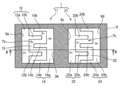
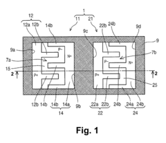
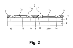
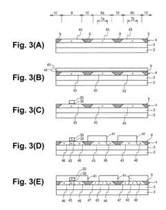
Innovation
- A photodiode design with a photosensitive element featuring a low concentration diffusion layer and high concentration P-type and N-type diffusion layers, where the P-type high concentration diffusion layer faces the N-type high concentration diffusion layer with the low concentration diffusion layer in between, and a method involving selective etching to reduce the silicon semiconductor layer thickness in specific areas to minimize interference and dark current.
Photodiode and manufacturing method, sensor and sensing array
PatentInactiveUS20210313358A1
Innovation
- A photodiode structure with epitaxial layers and doped regions of varying potentials arranged from the edge to the geometric center, concentrating photogenerated carriers for efficient transmission and reducing delays.
Calibration Standards
Calibration standards play a crucial role in ensuring the accuracy and reliability of photodiodes used in high-precision laboratory instruments. These standards provide a reference point for measuring and adjusting the performance of photodiodes, enabling consistent and comparable results across different devices and laboratories.
The development of calibration standards for photodiodes involves a multi-faceted approach, incorporating both physical and electrical parameters. Primary calibration standards are typically maintained by national metrology institutes and are based on cryogenic radiometers, which offer the highest level of accuracy in optical power measurements. These primary standards are then used to calibrate secondary standards, which are more practical for routine use in laboratories and manufacturing environments.
One key aspect of photodiode calibration standards is spectral responsivity. This parameter describes the photodiode's sensitivity to different wavelengths of light and is critical for applications requiring precise measurements across a wide spectral range. Calibration standards for spectral responsivity often utilize tunable laser sources or monochromators to generate precise wavelengths of light, allowing for the characterization of photodiode response across the entire operational spectrum.
Linearity is another important factor addressed by calibration standards. High-precision instruments require photodiodes that maintain a linear response over a wide range of light intensities. Calibration standards for linearity typically employ a series of neutral density filters or precision optical attenuators to create a range of known light intensities. By comparing the photodiode's output to these known intensities, any deviations from linearity can be identified and corrected.
Temperature dependence is a critical consideration in photodiode performance, particularly for high-precision applications. Calibration standards often include temperature-controlled environments to characterize how a photodiode's response changes with temperature. This information is essential for developing compensation algorithms or selecting photodiodes with minimal temperature sensitivity for specific applications.
Uniformity of response across the active area of the photodiode is another parameter addressed by calibration standards. This is particularly important for applications where the light spot size or position may vary. Standards for uniformity testing often employ precision translation stages to scan a small, well-defined light spot across the photodiode's surface, mapping out any variations in sensitivity.
Traceability is a fundamental principle in calibration standards, ensuring that measurements can be linked back to internationally recognized standards. For photodiodes, this often involves a chain of comparisons leading back to primary standards based on cryogenic radiometers. Maintaining and documenting this traceability is essential for ensuring the validity and comparability of measurements across different laboratories and over time.
Environmental Factors
Environmental factors play a crucial role in the performance and reliability of photodiodes used in high-precision laboratory instruments. These factors can significantly impact the accuracy and consistency of measurements, making it essential to consider and mitigate their effects during instrument design and operation.
Temperature fluctuations are one of the most critical environmental factors affecting photodiode performance. Changes in temperature can alter the semiconductor properties of the photodiode, leading to variations in dark current, responsivity, and spectral response. In high-precision applications, even small temperature-induced changes can result in measurement errors. To address this issue, temperature stabilization techniques, such as thermoelectric cooling or precise temperature control systems, are often employed to maintain a constant operating temperature for the photodiode.
Humidity is another environmental factor that can impact photodiode performance, particularly in long-term stability and reliability. High humidity levels can lead to condensation on the photodiode surface or within the device package, potentially causing corrosion, electrical leakage, or changes in optical properties. Proper hermetic sealing and the use of desiccants within the photodiode package can help mitigate humidity-related issues.
Electromagnetic interference (EMI) and radio frequency interference (RFI) can introduce noise and distortions in photodiode signals, especially in sensitive laboratory environments. Shielding techniques, such as Faraday cages or proper grounding, are often necessary to minimize the impact of external electromagnetic fields on photodiode performance.
Mechanical vibrations and shocks can affect the alignment and stability of optical components in laboratory instruments, potentially leading to measurement errors or damage to the photodiode. Vibration isolation systems and shock-absorbing mounts are commonly used to protect sensitive photodiode-based instruments from mechanical disturbances.
Ambient light is a significant concern for photodiode applications, as it can introduce unwanted background signals and reduce the signal-to-noise ratio. Light-tight enclosures, optical filters, and modulation techniques are often employed to minimize the impact of ambient light on photodiode measurements.
Dust and particulate contamination can degrade the optical performance of photodiodes by scattering or absorbing incident light. Clean room environments, protective windows, and regular cleaning procedures are essential for maintaining the optical integrity of photodiodes in high-precision instruments.
Atmospheric pressure variations can affect the performance of some types of photodiodes, particularly those used in gas sensing applications or instruments that rely on precise optical path lengths. Pressure-compensated designs or calibration techniques may be necessary to account for these effects in certain laboratory settings.
Unlock deeper insights with Patsnap Eureka Quick Research — get a full tech report to explore trends and direct your research. Try now!
Generate Your Research Report Instantly with AI Agent
Supercharge your innovation with Patsnap Eureka AI Agent Platform!