Advanced signal filtering in photodiode electronics
AUG 21, 20259 MIN READ
Generate Your Research Report Instantly with AI Agent
Patsnap Eureka helps you evaluate technical feasibility & market potential.
Signal Filtering Evolution and Objectives
Signal filtering in photodiode electronics has undergone significant evolution over the past decades, driven by the increasing demand for high-performance optical sensing and communication systems. The journey began with simple analog filters, progressing through various stages of sophistication to meet the ever-growing requirements for sensitivity, speed, and noise reduction in photodetector applications.
In the early stages, passive RC filters were commonly used to remove high-frequency noise from photodiode signals. These filters, while simple and cost-effective, had limitations in terms of bandwidth and roll-off characteristics. As technology advanced, active filters using operational amplifiers became prevalent, offering improved performance and flexibility in filter design.
The advent of digital signal processing (DSP) marked a significant milestone in signal filtering for photodiode electronics. DSP techniques allowed for more complex and adaptive filtering algorithms, enabling real-time adjustment of filter parameters based on signal characteristics. This development opened up new possibilities for dynamic noise reduction and signal enhancement in various applications, from scientific instrumentation to telecommunications.
Recent years have seen the integration of advanced filtering techniques directly into photodiode readout integrated circuits (ROICs). These on-chip filters combine analog and digital processing elements to achieve optimal signal conditioning at the source. Such integration has led to improved signal-to-noise ratios, reduced power consumption, and enhanced overall system performance.
The objectives of advanced signal filtering in photodiode electronics are multifaceted and continue to evolve. One primary goal is to push the boundaries of detection sensitivity, enabling the measurement of ever-weaker optical signals. This is particularly crucial in applications such as low-light imaging, spectroscopy, and long-range optical communication.
Another key objective is to increase the bandwidth of photodiode systems without compromising signal integrity. As data rates in optical communications continue to rise, filters must adapt to handle higher frequencies while effectively suppressing noise and inter-symbol interference.
Reducing the impact of environmental factors on signal quality remains a constant challenge. Advanced filtering techniques aim to mitigate the effects of temperature variations, electromagnetic interference, and other external disturbances that can degrade photodiode performance.
Looking forward, the field of signal filtering in photodiode electronics is set to embrace emerging technologies such as machine learning and artificial intelligence. These approaches promise to deliver adaptive filtering solutions that can learn and optimize their performance based on real-world data, potentially revolutionizing the way we process optical signals in diverse applications ranging from autonomous vehicles to quantum communication systems.
Market Demand Analysis for Advanced Filtering
The market demand for advanced signal filtering in photodiode electronics has been experiencing significant growth in recent years. This surge is primarily driven by the increasing adoption of photodiodes in various industries, including telecommunications, healthcare, automotive, and consumer electronics. As these sectors continue to evolve and demand higher performance from their optical sensing systems, the need for more sophisticated signal filtering techniques has become paramount.
In the telecommunications industry, the push towards higher data transmission rates and the implementation of 5G networks have created a strong demand for advanced filtering solutions. Photodiodes used in optical communication systems require precise signal processing to maintain signal integrity over long distances and in the presence of noise. This has led to a growing market for advanced filtering technologies that can effectively remove unwanted noise and interference from photodiode signals.
The healthcare sector has also emerged as a significant driver of demand for advanced signal filtering in photodiode electronics. Medical imaging systems, such as CT scanners and X-ray machines, rely heavily on photodiodes for accurate detection of radiation. As these systems become more sophisticated and require higher resolution imaging, the need for advanced filtering techniques to improve signal-to-noise ratios and enhance image quality has increased substantially.
In the automotive industry, the rise of advanced driver assistance systems (ADAS) and autonomous vehicles has created a new market for high-performance photodiode sensors. These sensors are crucial for applications such as LiDAR and object detection, where accurate and noise-free signal processing is essential for safety and reliability. The demand for advanced filtering solutions in this sector is expected to grow rapidly as autonomous vehicle technology continues to mature.
Consumer electronics represent another significant market for advanced signal filtering in photodiode electronics. With the increasing integration of optical sensors in smartphones, tablets, and wearable devices, there is a growing need for compact and efficient filtering solutions. These devices often operate in challenging environments with varying light conditions, necessitating advanced filtering techniques to ensure accurate and reliable sensor performance.
The industrial automation sector is also contributing to the market demand for advanced filtering solutions. As factories become more automated and rely on optical sensors for quality control and process monitoring, the need for precise and noise-resistant signal processing has increased. Advanced filtering techniques are essential for maintaining high levels of accuracy and reliability in these industrial applications.
Overall, the market demand for advanced signal filtering in photodiode electronics is driven by the need for improved performance, higher accuracy, and increased reliability across multiple industries. As technology continues to advance and new applications for photodiodes emerge, the demand for sophisticated filtering solutions is expected to grow further, creating opportunities for innovation and market expansion in this field.
Current Challenges in Photodiode Signal Processing
Photodiode signal processing faces several significant challenges in the current technological landscape. One of the primary issues is the presence of noise in the electrical signal generated by photodiodes. This noise can originate from various sources, including thermal noise, shot noise, and environmental electromagnetic interference. These unwanted fluctuations can severely degrade the signal-to-noise ratio (SNR), making it difficult to accurately detect and measure weak optical signals.
Another critical challenge is the limited dynamic range of photodiode systems. As the intensity of incident light varies over several orders of magnitude, the photodiode's response may become non-linear, leading to signal distortion or saturation. This limitation restricts the ability to accurately measure both very weak and very strong optical signals simultaneously, which is crucial in applications such as spectroscopy and optical communication.
The speed of signal processing is also a significant concern, particularly in high-speed applications like optical data transmission. As data rates continue to increase, the need for faster signal processing becomes more pressing. However, achieving high-speed operation while maintaining signal integrity and low noise levels presents a complex trade-off that engineers must carefully navigate.
Furthermore, the integration of photodiode systems with other electronic components poses challenges in terms of impedance matching and signal coupling. Improper integration can lead to signal reflections, distortions, and loss of bandwidth, compromising the overall system performance.
Temperature sensitivity is another critical issue in photodiode signal processing. Fluctuations in ambient temperature can affect the photodiode's dark current and responsivity, leading to measurement errors and drift in the output signal. Compensating for these temperature-induced variations requires sophisticated calibration and correction techniques.
Lastly, the miniaturization of photodiode systems for portable and integrated applications presents challenges in maintaining high performance within constrained power and space budgets. Balancing the need for advanced signal processing capabilities with low power consumption and small form factors requires innovative circuit design and optimization techniques.
Addressing these challenges requires a multifaceted approach, combining advancements in photodiode materials, circuit design, and signal processing algorithms. As the demand for more sensitive, faster, and more reliable photodiode systems continues to grow across various industries, overcoming these obstacles remains a key focus of research and development efforts in the field of optoelectronics.
State-of-the-Art Signal Filtering Techniques
01 Noise reduction in photodiode circuits
Various techniques are employed to reduce noise in photodiode circuits, including the use of low-noise amplifiers, filtering circuits, and shielding. These methods help to improve the signal-to-noise ratio and enhance the overall performance of photodiode-based systems.- Signal filtering techniques for photodiode output: Various signal filtering techniques are employed to process and improve the output from photodiodes. These methods aim to reduce noise, enhance signal quality, and increase the overall sensitivity of the photodiode system. Common approaches include low-pass filters, high-pass filters, and band-pass filters, which can be implemented using analog or digital circuits.
- Analog-to-digital conversion in photodiode circuits: Analog-to-digital converters (ADCs) are crucial components in photodiode electronics for signal processing. They convert the analog signal from the photodiode into a digital format for further processing or analysis. High-resolution ADCs are often used to maintain signal integrity and capture subtle variations in light intensity.
- Noise reduction techniques for photodiode signals: Various noise reduction techniques are implemented to improve the signal-to-noise ratio of photodiode outputs. These may include correlated double sampling, chopper stabilization, and active noise cancellation. Such methods help to minimize thermal noise, shot noise, and other sources of interference that can degrade the photodiode's performance.
- Integration of photodiodes with amplification circuits: Photodiodes are often integrated with amplification circuits to boost weak signals and improve overall sensitivity. These circuits may include transimpedance amplifiers, operational amplifiers, or specialized integrated circuits designed for photodiode applications. The amplification stage is crucial for enhancing the detectability of low-light signals and expanding the dynamic range of the photodiode system.
- Digital signal processing for photodiode output: Advanced digital signal processing techniques are applied to photodiode outputs to extract meaningful information and improve overall system performance. These may include adaptive filtering, Fourier transforms, wavelet analysis, and machine learning algorithms. Digital processing allows for more sophisticated analysis and can compensate for various non-idealities in the photodiode response.
02 Signal processing and filtering algorithms
Advanced signal processing and filtering algorithms are implemented to enhance the quality of photodiode output signals. These algorithms may include digital filtering, adaptive noise cancellation, and frequency domain analysis to extract meaningful information from raw photodiode data.Expand Specific Solutions03 Integration of photodiodes with readout circuits
Innovative designs integrate photodiodes with specialized readout circuits to optimize signal acquisition and processing. These integrated solutions often incorporate on-chip filtering and amplification stages to minimize external noise sources and improve overall system performance.Expand Specific Solutions04 Optical filtering for improved photodiode performance
Optical filtering techniques are applied to enhance photodiode performance by selectively transmitting desired wavelengths and rejecting unwanted light. This approach can significantly improve signal quality and reduce the need for extensive electronic filtering in certain applications.Expand Specific Solutions05 Time-gated photodiode systems
Time-gated photodiode systems are developed to improve signal detection in high-noise environments. By synchronizing the photodiode activation with the expected signal arrival time, these systems can effectively filter out background noise and enhance the detection of weak signals.Expand Specific Solutions
Key Players in Photodiode Electronics Industry
The advanced signal filtering in photodiode electronics market is in a growth phase, driven by increasing demand for high-precision sensing and detection applications. The market size is expanding, with significant potential in sectors like telecommunications, healthcare, and industrial automation. Technologically, the field is advancing rapidly, with companies like OSRAM Opto Semiconductors, Hamamatsu Photonics, and ams-OSRAM AG leading innovation. These firms are developing sophisticated filtering techniques and integrated solutions, pushing the boundaries of photodiode performance. The competitive landscape is diverse, featuring both established electronics giants and specialized optoelectronics companies, indicating a mature yet dynamic market with ongoing technological evolution.
OSRAM Opto Semiconductors GmbH
Technical Solution: OSRAM Opto Semiconductors has developed cutting-edge signal filtering techniques for photodiode electronics, with a focus on high-performance optical sensing in automotive and industrial applications. Their approach includes the use of advanced epitaxial structures to optimize quantum efficiency and reduce dark current, combined with integrated signal processing circuits. OSRAM has implemented innovative package designs that minimize parasitic capacitance, allowing for faster response times and improved signal quality. Their photodiodes often feature built-in temperature compensation circuits, maintaining stable performance across a wide temperature range of -40°C to +125°C [5]. OSRAM's solutions also incorporate advanced optical filters directly integrated into the chip, achieving narrowband spectral responses with full-width half-maximum (FWHM) values as low as 20 nm [6].
Strengths: Excellent performance in harsh environments, high integration level, and optimized for specific application needs. Weaknesses: Potentially higher cost for specialized solutions, may have limited flexibility for general-purpose applications.
Agilent Technologies, Inc.
Technical Solution: Agilent Technologies has developed sophisticated signal filtering techniques for photodiode electronics, focusing on high-precision measurement and analysis applications. Their approach includes the use of ultra-low noise amplification circuits combined with advanced digital signal processing algorithms. Agilent has implemented adaptive filtering techniques that can automatically adjust to changing signal conditions, improving measurement accuracy and dynamic range. Their solutions often incorporate high-resolution analog-to-digital converters (ADCs) with sampling rates up to 1 GSPS, allowing for detailed analysis of fast transient signals [7]. Agilent's photodiode systems feature proprietary calibration and correction algorithms that can compensate for temperature drift and aging effects, maintaining measurement accuracy over time [8].
Strengths: Exceptional measurement accuracy, advanced signal analysis capabilities, and long-term stability. Weaknesses: Higher cost due to precision components, may be overspecified for simpler applications.
Innovative Approaches in Noise Reduction
Circuit arrangement for supplying a photodiode with a bias
PatentWO2007033809A1
Innovation
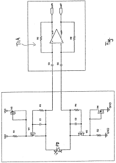
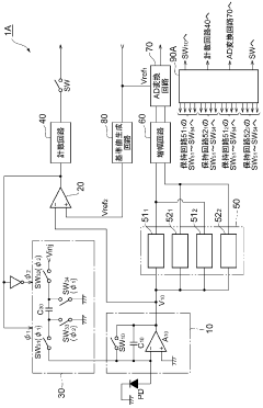
- A circuit arrangement that uses a current control device with a low-pass filter connected to the photodiode, stabilized by negative feedback, to maintain a stable bias voltage, reducing noise and allowing detection of higher-frequency signals while suppressing interference. This includes MOS transistors for low current control and parasitic capacitance-based low-pass filtering, along with a transimpedance amplifier for improved signal-to-noise ratio.
Signal processing device and photodetection device
PatentWO2010090135A1
Innovation
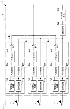
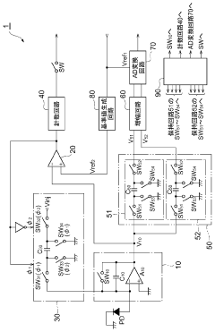
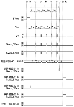
- A signal processing device with an integration circuit, comparison circuit, charge injection circuit, counting circuit, and AD conversion circuit that accumulates and converts photodiode charge into a digital signal, while a holding circuit and amplifier circuit enhance accuracy by isolating and amplifying the signal, reducing noise impact.
Electromagnetic Compatibility Considerations
Electromagnetic compatibility (EMC) is a critical consideration in the design and implementation of advanced signal filtering systems for photodiode electronics. The high sensitivity of photodiodes to electromagnetic interference (EMI) necessitates careful attention to EMC principles to ensure optimal performance and reliability.
In photodiode circuits, even small amounts of electromagnetic noise can significantly impact signal quality and measurement accuracy. This is particularly true in applications requiring high precision, such as optical communication systems, scientific instrumentation, and medical imaging devices. To address these challenges, several EMC strategies must be employed in the design of advanced signal filtering systems.
Shielding is a fundamental EMC technique that plays a crucial role in protecting photodiode circuits from external electromagnetic fields. Proper shielding involves enclosing sensitive components within conductive enclosures, effectively creating a Faraday cage. This approach helps to attenuate both radiated and conducted electromagnetic interference, preserving the integrity of the photodiode's output signal.
Grounding and power supply decoupling are essential aspects of EMC design in photodiode electronics. A well-designed grounding scheme minimizes ground loops and reduces common-mode noise. Implementing star-point grounding techniques and using low-impedance ground planes can significantly improve EMC performance. Additionally, careful placement of decoupling capacitors near active components helps to suppress high-frequency noise on power supply lines.
Printed circuit board (PCB) layout is another critical factor in achieving good EMC in photodiode circuits. Proper component placement and trace routing can minimize parasitic effects and reduce electromagnetic coupling between circuit elements. Techniques such as separating analog and digital grounds, using guard rings around sensitive components, and implementing differential signaling can greatly enhance EMC performance.
Filter design itself must also take EMC considerations into account. While the primary goal of advanced signal filtering is to extract the desired signal from noise, the filter components and topology can inadvertently act as sources or receptors of electromagnetic interference. Careful selection of filter components, such as using shielded inductors and low-ESR capacitors, can help mitigate these issues.
Compliance with relevant EMC standards and regulations is essential for commercial products incorporating photodiode electronics. Standards such as IEC 61000 series for electromagnetic compatibility provide guidelines and test methods to ensure that electronic equipment meets specified EMC requirements. Adhering to these standards not only ensures regulatory compliance but also contributes to the overall robustness and reliability of the photodiode system.
Performance Metrics and Standardization
In the realm of advanced signal filtering for photodiode electronics, establishing robust performance metrics and standardization is crucial for ensuring consistent and reliable signal processing across various applications. These metrics serve as benchmarks for evaluating the effectiveness of filtering techniques and enable meaningful comparisons between different systems.
Key performance metrics for signal filtering in photodiode electronics typically include signal-to-noise ratio (SNR), bandwidth, dynamic range, and response time. SNR is particularly important as it quantifies the ability of the filtering system to extract the desired signal from background noise. Higher SNR values indicate better filter performance and cleaner output signals. Bandwidth measurements assess the range of frequencies that can be effectively processed, which is critical for applications requiring high-speed data acquisition or wide spectral sensitivity.
Dynamic range, expressed in decibels, represents the ratio between the largest and smallest signals that can be accurately processed. This metric is essential for applications involving varying light intensities or rapid changes in illumination. Response time, measured in nanoseconds or microseconds, indicates how quickly the filtering system can react to changes in the input signal, which is crucial for time-sensitive applications such as high-speed imaging or optical communication systems.
Standardization efforts in this field aim to establish common testing procedures and performance criteria, ensuring consistency across different manufacturers and applications. Organizations such as the International Electrotechnical Commission (IEC) and the Institute of Electrical and Electronics Engineers (IEEE) play pivotal roles in developing and maintaining these standards. For instance, the IEC 60747-5 standard provides guidelines for measuring and specifying the characteristics of optoelectronic devices, including photodiodes and their associated electronics.
These standards typically define test conditions, measurement methodologies, and reporting formats for key performance parameters. They may specify reference light sources, environmental conditions, and electrical load requirements to ensure reproducible results. Additionally, standards often address issues such as long-term stability, temperature dependence, and linearity of response, which are critical for maintaining consistent performance in real-world applications.
As the field of photodiode electronics continues to advance, performance metrics and standardization efforts must evolve to keep pace with emerging technologies and applications. This includes developing new metrics for evaluating advanced filtering techniques such as adaptive filters, machine learning-based approaches, and integrated photonic circuits. Future standards may also need to address the unique challenges posed by novel photodiode materials and structures, such as graphene-based detectors or quantum dot photodiodes.
Unlock deeper insights with Patsnap Eureka Quick Research — get a full tech report to explore trends and direct your research. Try now!
Generate Your Research Report Instantly with AI Agent
Supercharge your innovation with Patsnap Eureka AI Agent Platform!