Advancements in photodiode materials for infrared imaging
AUG 21, 20259 MIN READ
Generate Your Research Report Instantly with AI Agent
Patsnap Eureka helps you evaluate technical feasibility & market potential.
IR Imaging Evolution
Infrared (IR) imaging technology has undergone significant evolution since its inception, driven by advancements in photodiode materials and sensor technologies. The journey of IR imaging can be traced back to the 1940s when the first thermal imaging devices were developed for military applications. These early systems were bulky, expensive, and limited in their capabilities.
The 1960s and 1970s saw the emergence of cooled IR detectors, which offered improved sensitivity and image quality. However, these systems required cryogenic cooling, making them impractical for widespread use. The development of uncooled microbolometer technology in the 1980s marked a significant milestone in IR imaging evolution, enabling the production of more compact and cost-effective thermal cameras.
The 1990s witnessed a surge in research and development of new photodiode materials for IR imaging. Indium gallium arsenide (InGaAs) emerged as a promising material for near-infrared (NIR) and short-wave infrared (SWIR) imaging, offering enhanced sensitivity and lower noise compared to traditional silicon-based detectors. This period also saw the introduction of quantum well infrared photodetectors (QWIPs), which expanded the spectral range of IR imaging systems.
The turn of the millennium brought about rapid advancements in IR imaging technology. The development of mercury cadmium telluride (HgCdTe) detectors revolutionized long-wave infrared (LWIR) imaging, providing superior performance in terms of sensitivity and operating temperature. Simultaneously, improvements in microbolometer technology led to the widespread adoption of uncooled thermal cameras in various applications, including surveillance, automotive, and industrial inspection.
In recent years, the focus has shifted towards developing novel photodiode materials and structures to enhance IR imaging capabilities. Type-II superlattice (T2SL) detectors have emerged as a promising alternative to HgCdTe, offering comparable performance with potential advantages in manufacturability and cost. Additionally, research into two-dimensional materials such as graphene and black phosphorus has opened up new possibilities for ultra-thin, flexible IR detectors.
The evolution of IR imaging has also been characterized by the integration of advanced signal processing and machine learning algorithms. These computational techniques have enabled significant improvements in image quality, resolution, and object recognition capabilities, further expanding the application scope of IR imaging systems.
Looking ahead, the future of IR imaging is poised for continued innovation. Emerging trends include the development of multi-spectral and hyperspectral imaging systems, which can provide more detailed information about the composition and properties of objects in a scene. Additionally, ongoing research into novel nanomaterials and quantum dot structures holds promise for next-generation IR detectors with enhanced performance and functionality.
Market Demand Analysis
The market demand for advanced photodiode materials in infrared imaging has been experiencing significant growth, driven by various factors across multiple industries. The increasing adoption of infrared imaging technology in consumer electronics, particularly in smartphones and wearable devices, has created a substantial market opportunity. This trend is expected to continue as manufacturers seek to incorporate more sophisticated sensing capabilities into their products.
In the automotive sector, the demand for infrared imaging systems has surged due to the development of advanced driver assistance systems (ADAS) and autonomous vehicles. These systems rely heavily on infrared sensors for night vision, pedestrian detection, and obstacle avoidance, creating a robust market for high-performance photodiode materials.
The security and surveillance industry has also been a major contributor to the growing demand for infrared imaging technology. Government agencies, commercial enterprises, and residential consumers are increasingly investing in infrared-enabled security cameras and thermal imaging systems, driving the need for more sensitive and efficient photodiode materials.
In the healthcare sector, infrared imaging has found applications in medical diagnostics, such as early detection of diseases and non-invasive temperature monitoring. This has led to an increased demand for high-resolution infrared sensors, further fueling the market for advanced photodiode materials.
The aerospace and defense industries continue to be significant consumers of infrared imaging technology, with applications ranging from target acquisition and tracking to thermal surveillance and reconnaissance. The need for enhanced night vision capabilities and long-range detection systems has driven the demand for more sophisticated photodiode materials in this sector.
Industrial applications, including predictive maintenance, process monitoring, and quality control, have also contributed to the growing market for infrared imaging technology. The ability to detect heat signatures and identify potential equipment failures has made infrared cameras invaluable tools in manufacturing and energy production facilities.
As environmental concerns gain prominence, there has been an increased focus on energy efficiency and building management. This has led to a rising demand for infrared imaging systems in thermal mapping and energy audits, creating additional market opportunities for advanced photodiode materials.
The global market for infrared imaging is projected to expand at a compound annual growth rate (CAGR) of over 7% in the coming years. This growth is expected to be driven by technological advancements in photodiode materials, which will enable the development of more sensitive, compact, and cost-effective infrared sensors. As a result, the demand for innovative materials that can enhance the performance and reduce the cost of infrared imaging systems is likely to remain strong across various industries.
Photodiode Challenges
Despite significant advancements in photodiode technology for infrared imaging, several challenges persist in the development and implementation of these materials. One of the primary obstacles is the trade-off between sensitivity and operating temperature. High-performance infrared photodiodes often require cryogenic cooling to achieve optimal sensitivity and reduce thermal noise, which significantly increases system complexity and cost.
Material defects and impurities pose another significant challenge in photodiode fabrication. These imperfections can lead to increased dark current, reduced quantum efficiency, and overall degradation of device performance. Achieving high-quality, uniform material growth across large areas remains a technical hurdle, particularly for compound semiconductors used in long-wavelength infrared detection.
The spectral response of photodiode materials presents an ongoing challenge. While some materials excel in specific wavelength ranges, developing broadband detectors that can efficiently capture a wide range of infrared wavelengths is still an area of active research. This limitation often necessitates the use of multiple detectors or complex optical systems to cover the desired spectral range.
Stability and reliability of photodiode materials under various operating conditions are critical concerns. Environmental factors such as temperature fluctuations, humidity, and radiation exposure can lead to material degradation over time, affecting long-term performance and reliability. Developing robust materials that maintain their properties under harsh conditions is essential for many applications, particularly in space-based and industrial imaging systems.
Integration challenges also persist, especially when incorporating advanced photodiode materials into existing readout integrated circuits (ROICs) and imaging systems. Compatibility issues between novel materials and standard semiconductor processing techniques can limit the scalability and manufacturability of new photodiode technologies.
Cost remains a significant barrier to widespread adoption of advanced photodiode materials. Many high-performance materials, such as mercury cadmium telluride (MCT), are expensive to produce and process, limiting their use to specialized applications. Finding cost-effective alternatives or improving manufacturing processes for existing materials is crucial for expanding the market for infrared imaging technologies.
Lastly, the pursuit of higher pixel densities and smaller pixel sizes in infrared focal plane arrays (FPAs) introduces new challenges in material design and fabrication. As pixel dimensions shrink, maintaining high quantum efficiency and low crosstalk becomes increasingly difficult, requiring innovative approaches to material growth and device architecture.
Current PD Solutions
01 Silicon-based photodiode materials
Silicon is a widely used material for photodiodes due to its high sensitivity in the visible and near-infrared spectrum. Silicon photodiodes offer good quantum efficiency, low dark current, and fast response times. Various doping techniques and structural modifications can be applied to enhance their sensitivity and spectral range.- Silicon-based photodiode materials: Silicon is a widely used material for photodiodes due to its high sensitivity in the visible and near-infrared spectrum. Silicon photodiodes offer good quantum efficiency, low dark current, and fast response times. Various doping techniques and structural modifications can be applied to enhance their sensitivity and performance.
- III-V compound semiconductor photodiodes: III-V compound semiconductors, such as GaAs, InGaAs, and InP, are used to fabricate high-performance photodiodes. These materials offer excellent sensitivity in the near-infrared and infrared regions, making them suitable for applications in optical communications and spectroscopy. They can be engineered to have specific bandgaps and absorption characteristics.
- Avalanche photodiodes (APDs): Avalanche photodiodes are designed to provide internal gain through impact ionization. This results in higher sensitivity and improved signal-to-noise ratio compared to conventional photodiodes. APDs are particularly useful in low-light conditions and high-speed applications. Materials such as silicon and III-V compounds can be used to fabricate APDs with different performance characteristics.
- Organic and perovskite photodiode materials: Organic and perovskite materials are emerging as promising candidates for photodiode applications. These materials offer advantages such as flexibility, low-cost fabrication, and tunable optical properties. Organic photodiodes can be designed to have high sensitivity in specific wavelength ranges, while perovskite-based devices show potential for high-performance, solution-processable photodetectors.
- Nanostructured photodiode materials: Nanostructured materials, such as quantum dots, nanowires, and 2D materials, are being explored to enhance photodiode sensitivity. These structures can offer unique optical and electronic properties, including increased light absorption, carrier multiplication, and improved charge transport. Nanostructured photodiodes have the potential to achieve high sensitivity across a wide spectral range.
02 III-V compound semiconductor photodiodes
III-V compound semiconductors, such as InGaAs, GaAs, and InP, are used to fabricate high-performance photodiodes. These materials offer excellent sensitivity in the near-infrared to mid-infrared range, making them suitable for applications in optical communications and spectroscopy. They can be engineered to have specific bandgaps and absorption characteristics.Expand Specific Solutions03 Avalanche photodiodes (APDs)
Avalanche photodiodes are designed to provide internal gain through impact ionization. This results in higher sensitivity compared to conventional photodiodes, especially in low-light conditions. APDs are typically made from materials like silicon, InGaAs, or germanium, and their sensitivity can be further enhanced by optimizing the avalanche region and reducing noise.Expand Specific Solutions04 Organic and perovskite photodiode materials
Organic and perovskite materials are emerging as promising candidates for photodiodes. These materials offer advantages such as low-cost fabrication, flexibility, and tunable optical properties. Research is focused on improving their sensitivity, stability, and spectral response range for various applications, including image sensors and solar cells.Expand Specific Solutions05 Nanostructured photodiode materials
Nanostructured materials, such as quantum dots, nanowires, and 2D materials, are being explored to enhance photodiode sensitivity. These structures can offer benefits like increased light absorption, improved carrier collection, and tailored spectral response. Integration of nanostructures with conventional photodiode materials can lead to higher sensitivity and expanded functionality.Expand Specific Solutions
Key Industry Players
The advancements in photodiode materials for infrared imaging are progressing rapidly, with the industry in a growth phase characterized by increasing market size and evolving technological maturity. Major players like FUJIFILM Corp., Sumitomo Electric Industries Ltd., and Nichia Corp. are driving innovation in this field. The market is expanding due to growing applications in automotive, healthcare, and consumer electronics sectors. While established companies are refining existing technologies, emerging firms like W&Wsens Devices, Inc. are introducing novel approaches, such as thin silicon photosensors with high NIR sensitivity. This competitive landscape is fostering rapid technological progress, with a focus on improving sensitivity, resolution, and cost-effectiveness of infrared imaging solutions.
FUJIFILM Corp.
Technical Solution: FUJIFILM has made significant advancements in photodiode materials for infrared imaging, particularly focusing on organic photodiodes (OPDs). Their approach involves developing novel organic semiconductor materials with enhanced near-infrared (NIR) sensitivity. FUJIFILM has successfully created OPDs with a spectral response extending beyond 1000 nm, utilizing specially designed donor-acceptor copolymers[1]. These materials exhibit improved charge carrier mobility and broader absorption spectra, resulting in higher quantum efficiency in the NIR region. Additionally, FUJIFILM has implemented a bulk heterojunction structure in their OPDs, which enhances charge separation and collection, leading to improved responsivity and lower dark current[2].
Strengths: High NIR sensitivity, potential for flexible and large-area sensors, cost-effective solution for IR imaging. Weaknesses: Stability and lifetime of organic materials may be inferior to inorganic alternatives, potential limitations in extreme temperature environments.
Samsung Electronics Co., Ltd.
Technical Solution: Samsung has been pioneering advancements in photodiode materials for infrared imaging, focusing on quantum dot (QD) based photodetectors. Their approach involves synthesizing colloidal quantum dots with precisely controlled size and composition to tune the absorption spectrum into the infrared region. Samsung has developed lead sulfide (PbS) and mercury telluride (HgTe) QDs with high absorption coefficients in the short-wave infrared (SWIR) range[3]. These QDs are integrated into solution-processed thin films, enabling cost-effective and large-area fabrication of infrared photodetectors. Samsung has also implemented ligand exchange techniques to enhance charge transport between QDs, resulting in improved responsivity and detectivity[4]. Furthermore, they have explored the use of core-shell QD structures to reduce surface defects and enhance photostability.
Strengths: Tunable absorption spectrum, potential for low-cost and large-area fabrication, high absorption coefficients. Weaknesses: Potential toxicity of some QD materials, challenges in long-term stability and uniformity of QD films.
Core PD Innovations
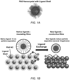
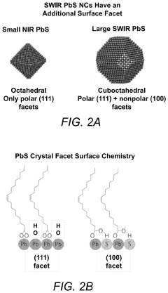
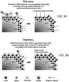
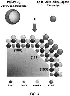
Enhanced Infrared Photodiodes Based on PbS/PbClx Core/Shell Nanocrystals
PatentInactiveUS20220020942A1
Innovation
- The use of PbS/PbClx core/shell nanocrystals, where a PbClx shell layer provides native halide passivation to the (100) surfaces, allowing for complete surface passivation and enabling established halide ligand exchange protocols, thereby improving charge carrier mobility and reducing surface defects.
Infrared photodiode and sensor and electronic device
PatentPendingUS20230015790A1
Innovation
- An infrared photodiode with a photoelectric conversion layer incorporating an infrared absorbing material and a counter material forming a pn junction, configured to exhibit external quantum efficiency in the wavelength region of 1000 nm to 3000 nm, utilizing a microcavity structure and specific layer thicknesses and composition ratios to enhance absorption beyond the limitations of silicon photodiodes.
Material Science Impact
The impact of material science on advancements in photodiode materials for infrared imaging has been profound and far-reaching. The development of novel materials and innovative fabrication techniques has significantly enhanced the performance and capabilities of infrared imaging systems.
One of the most significant contributions of material science has been the creation of new semiconductor materials with tailored bandgaps. These materials, such as mercury cadmium telluride (HgCdTe) and indium gallium arsenide (InGaAs), have enabled the detection of infrared radiation across a wider range of wavelengths. By precisely controlling the composition and structure of these materials, researchers have been able to optimize their optical and electrical properties for specific infrared imaging applications.
Nanostructured materials have also played a crucial role in advancing photodiode technology. Quantum dots, nanowires, and two-dimensional materials like graphene have been incorporated into photodiode designs, leading to improved sensitivity and faster response times. These nanomaterials offer unique quantum confinement effects and high carrier mobility, which translate into enhanced device performance.
Material science has also contributed to the development of novel device architectures. For instance, the introduction of multi-junction photodiodes has allowed for the simultaneous detection of different infrared wavelengths, enabling multispectral imaging capabilities. Additionally, the integration of plasmonic structures and metamaterials has led to increased light absorption and improved quantum efficiency in photodiodes.
Advancements in thin-film deposition techniques and epitaxial growth processes have enabled the fabrication of high-quality, uniform photodiode arrays with improved yield and reduced defects. These manufacturing improvements have been instrumental in scaling up production and reducing costs, making infrared imaging technology more accessible for various applications.
The development of new passivation materials and surface treatments has significantly reduced dark current and noise in photodiodes, leading to improved signal-to-noise ratios and enhanced image quality. This has been particularly important for low-light imaging and long-wavelength infrared detection.
Material science has also contributed to the creation of flexible and stretchable photodiodes, opening up new possibilities for wearable and conformal infrared imaging devices. By combining novel organic and inorganic materials with innovative fabrication techniques, researchers have developed photodiodes that can maintain their performance under mechanical stress and deformation.
In conclusion, the field of material science has been instrumental in driving advancements in photodiode materials for infrared imaging. Through the development of new materials, device architectures, and fabrication techniques, material scientists have significantly improved the performance, versatility, and applicability of infrared imaging systems across various industries and research domains.
Thermal Imaging Apps
Thermal imaging applications have expanded significantly with advancements in photodiode materials for infrared imaging. These applications now span various sectors, including industrial, medical, automotive, and consumer electronics.
In the industrial sector, thermal imaging is widely used for predictive maintenance and quality control. Manufacturing facilities employ infrared cameras to detect overheating equipment, identify potential failures, and optimize energy efficiency. The improved sensitivity and resolution of modern photodiode materials allow for more accurate temperature measurements and early detection of anomalies in production processes.
The medical field has seen a surge in thermal imaging applications, particularly in diagnostic and screening procedures. Infrared cameras are used for detecting fever, a key symptom in many infectious diseases. The non-invasive nature of thermal imaging makes it an attractive option for mass screening in public spaces. Additionally, thermal imaging aids in the diagnosis of circulatory disorders, inflammation, and certain types of cancer by detecting subtle temperature variations in the body.
In the automotive industry, thermal imaging is becoming increasingly important for enhancing driver safety. Night vision systems using infrared cameras can detect pedestrians, animals, and obstacles in low-light conditions, significantly reducing the risk of accidents. Advanced driver assistance systems (ADAS) incorporate thermal imaging to improve object detection and classification, complementing traditional visible light cameras and radar systems.
The consumer electronics market has also embraced thermal imaging technology. Smartphones with integrated thermal cameras are now available, allowing users to perform basic home inspections, detect heat leaks, and even assist in cooking. Outdoor enthusiasts use handheld thermal imagers for wildlife observation and navigation in low-visibility conditions.
Security and surveillance applications have greatly benefited from improvements in photodiode materials. High-resolution thermal cameras can detect intruders in complete darkness, making them invaluable for perimeter security in both military and civilian settings. Border control and law enforcement agencies use thermal imaging for search and rescue operations and to track suspects in challenging environments.
In agriculture, thermal imaging drones are employed to monitor crop health, detect irrigation issues, and identify areas of pest infestation. The ability to capture large-scale thermal data quickly and efficiently has revolutionized precision agriculture practices.
As photodiode materials continue to advance, we can expect to see further miniaturization and cost reduction of thermal imaging devices. This will likely lead to even broader adoption across industries and the development of novel applications that leverage the unique capabilities of infrared imaging technology.
Unlock deeper insights with Patsnap Eureka Quick Research — get a full tech report to explore trends and direct your research. Try now!
Generate Your Research Report Instantly with AI Agent
Supercharge your innovation with Patsnap Eureka AI Agent Platform!