

Photodiode reflection reduction through surface texturing
AUG 21, 20259 MIN READ
Generate Your Research Report Instantly with AI Agent
PatSnap Eureka helps you evaluate technical feasibility & market potential.
Photodiode Texturing Background and Objectives
Photodiodes have been a cornerstone of optoelectronic technology for decades, playing crucial roles in various applications ranging from telecommunications to medical imaging. The evolution of photodiode technology has been driven by the constant pursuit of higher sensitivity, faster response times, and improved signal-to-noise ratios. One of the persistent challenges in photodiode design has been the reduction of unwanted reflections from the device surface, which can significantly impact performance.
Surface texturing has emerged as a promising approach to address this issue, offering the potential to dramatically reduce reflections and enhance overall photodiode efficiency. This technique involves modifying the surface structure of the photodiode at the micro or nanoscale to manipulate how light interacts with the device. The concept draws inspiration from nature, where examples like moth eyes demonstrate remarkable anti-reflective properties due to their unique surface structures.
The primary objective of photodiode texturing is to minimize the amount of light reflected from the device surface, thereby increasing the amount of light absorbed and converted into electrical signals. This goal aligns with the broader aim of improving photodiode performance across various metrics, including quantum efficiency, responsivity, and detection limits. By reducing reflections, texturing can potentially enhance the sensitivity of photodiodes, particularly in low-light conditions or when detecting weak signals.
Another key objective is to achieve these improvements while maintaining or enhancing other critical photodiode characteristics. This includes preserving or improving the device's spectral response, ensuring compatibility with existing manufacturing processes, and maintaining long-term reliability under various operating conditions. The challenge lies in optimizing the surface texture to achieve the desired anti-reflective properties without compromising other aspects of photodiode performance or significantly increasing production costs.
The development of effective texturing techniques for photodiodes is driven by the increasing demands of emerging technologies. Fields such as LiDAR for autonomous vehicles, high-speed optical communications, and advanced scientific instrumentation all require photodiodes with exceptional performance characteristics. As these applications push the boundaries of what is possible with current photodiode technology, the need for innovative solutions like surface texturing becomes more pressing.
Understanding the historical context and current objectives of photodiode texturing is crucial for guiding future research and development efforts. This technology has the potential to not only enhance existing applications but also enable new use cases that were previously impractical due to performance limitations. As such, the exploration of photodiode texturing represents a significant area of interest for both academic researchers and industry professionals seeking to advance the state of the art in optoelectronic devices.
Market Demand Analysis for Enhanced Photodiodes
The market demand for enhanced photodiodes, particularly those with reduced reflection through surface texturing, has been steadily increasing across various industries. This growth is primarily driven by the expanding applications of photodiodes in sectors such as telecommunications, automotive, healthcare, and consumer electronics.
In the telecommunications industry, the demand for high-performance photodiodes is surging due to the rapid deployment of 5G networks and the increasing need for high-speed optical communication systems. Surface-textured photodiodes offer improved sensitivity and reduced noise, making them ideal for long-distance data transmission and high-bandwidth applications.
The automotive sector is another significant driver of market demand for enhanced photodiodes. With the rise of advanced driver-assistance systems (ADAS) and autonomous vehicles, there is a growing need for reliable and efficient light detection sensors. Surface-textured photodiodes provide better performance in varying light conditions, crucial for applications such as LiDAR systems and adaptive headlights.
In healthcare, the demand for enhanced photodiodes is fueled by advancements in medical imaging and diagnostic equipment. Surface-textured photodiodes offer improved sensitivity and reduced noise, enabling more accurate and detailed imaging in applications such as computed tomography (CT) scanners, X-ray detectors, and endoscopic devices.
The consumer electronics market is also contributing to the increased demand for enhanced photodiodes. As smartphones, tablets, and wearable devices incorporate more advanced sensing capabilities, there is a growing need for high-performance photodiodes in applications such as ambient light sensing, proximity detection, and biometric authentication.
Environmental monitoring and industrial automation sectors are emerging as potential growth areas for enhanced photodiodes. These industries require sensors with high sensitivity and reliability for applications such as air quality monitoring, process control, and safety systems.
The global market for photodiodes is expected to experience substantial growth in the coming years. This growth is attributed to the increasing adoption of IoT devices, smart home technologies, and the ongoing digital transformation across industries. Surface-textured photodiodes, with their improved performance characteristics, are well-positioned to capture a significant share of this expanding market.
However, challenges such as manufacturing complexity and cost considerations may impact the widespread adoption of surface-textured photodiodes. Overcoming these challenges through innovative manufacturing techniques and economies of scale will be crucial for meeting the growing market demand and realizing the full potential of this technology across various industries.
Current Challenges in Photodiode Reflection Reduction
Despite significant advancements in photodiode technology, reflection reduction remains a critical challenge in optimizing device performance. The primary issue stems from the inherent reflective properties of semiconductor materials used in photodiodes, which can lead to substantial light loss and reduced quantum efficiency.
One of the main obstacles in reflection reduction is achieving a balance between effective light trapping and maintaining the electrical properties of the photodiode. Surface texturing techniques, while promising, often introduce surface defects and increase recombination sites, potentially degrading the device's overall performance.
The complexity of designing optimal surface textures poses another significant challenge. The ideal texture pattern depends on various factors, including the wavelength of incident light, the refractive index of the semiconductor material, and the desired angular response of the photodiode. Developing a universal texturing solution that works across a broad spectrum of wavelengths and incident angles remains elusive.
Manufacturing constraints further complicate the implementation of advanced surface texturing techniques. Many promising nano-scale texturing methods are difficult to scale up for mass production, limiting their practical application in commercial photodiodes. The need for precise control over texture dimensions and uniformity across large areas presents significant fabrication challenges.
Additionally, the integration of textured surfaces with other photodiode components, such as antireflection coatings and passivation layers, introduces compatibility issues. Ensuring that surface texturing does not compromise the effectiveness of these additional layers or interfere with electrical contacts is a complex task that requires careful engineering.
The durability and long-term stability of textured surfaces in various operating environments is another concern. Exposure to harsh conditions, temperature fluctuations, and mechanical stress can potentially degrade the texture over time, reducing its effectiveness in reflection reduction.
Furthermore, the cost-effectiveness of implementing advanced surface texturing techniques remains a significant hurdle for widespread adoption. Many high-performance texturing methods require expensive equipment or complex processing steps, making them economically unfeasible for certain applications.
Lastly, the trade-off between reflection reduction and other performance metrics, such as dark current and response time, presents an ongoing challenge. Optimizing surface texture for maximum light absorption may inadvertently affect other critical parameters, necessitating a delicate balance in device design.
Existing Surface Texturing Solutions
01 Photodiode structure for improved reflection
Specialized photodiode structures are designed to enhance light reflection and absorption. These structures may include specific layer configurations, surface treatments, or geometric designs that optimize the capture of incident light, reducing unwanted reflections and improving overall sensitivity.- Photodiode structure for improved reflection: Specialized photodiode structures are designed to enhance light reflection and absorption. These structures may include specific layer configurations, surface treatments, or geometric designs that optimize the capture of incident light, reducing unwanted reflections and improving overall sensitivity.
- Anti-reflection coatings for photodiodes: Anti-reflection coatings are applied to photodiode surfaces to minimize light reflection and maximize absorption. These coatings typically consist of one or more thin layers of materials with specific refractive indices, designed to destructively interfere with reflected light waves and enhance transmission into the photodiode.
- Integration of photodiodes with optical elements: Photodiodes are integrated with various optical elements such as lenses, mirrors, or waveguides to control and optimize light reflection and collection. These integrated designs can improve the overall efficiency of light capture and reduce unwanted reflections in specific applications.
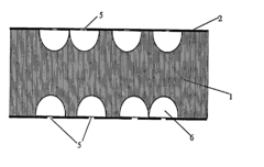
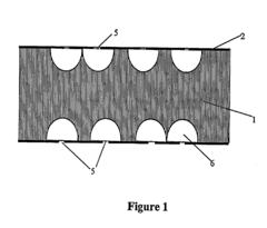
- Surface texturing for reflection control: The surface of photodiodes or associated optical components is textured to control light reflection. This can involve micro- or nano-scale patterns that scatter or trap light, reducing specular reflection and enhancing absorption. Various texturing techniques and patterns are employed to optimize performance for different wavelengths and applications.
- Reflection measurement and characterization: Methods and systems are developed for measuring and characterizing reflections from photodiode surfaces. These techniques help in evaluating the effectiveness of anti-reflection strategies and optimizing photodiode designs. They may involve specialized optical setups, signal processing algorithms, or calibration procedures to accurately quantify reflection properties.
02 Anti-reflection coatings for photodiodes
Anti-reflection coatings are applied to photodiode surfaces to minimize light reflection and maximize absorption. These coatings typically consist of one or more thin layers of materials with specific refractive indices, designed to create destructive interference of reflected light waves.Expand Specific Solutions03 Integration of photodiodes with optical elements
Photodiodes are integrated with various optical elements such as lenses, mirrors, or waveguides to control and optimize light reflection. These integrated designs can focus light onto the active area of the photodiode, redirect reflected light, or enhance light collection efficiency.Expand Specific Solutions04 Surface texturing for reflection control
The surface of photodiodes is textured or patterned to control light reflection. This can include micro- or nano-scale structures that scatter or trap light, reducing specular reflection and increasing the probability of light absorption within the device.Expand Specific Solutions05 Backside illumination and reflection management
Backside illumination techniques are employed in photodiode design to manage reflection and improve light sensitivity. This approach involves illuminating the photodiode from the back side of the substrate, often incorporating reflective layers or structures to redirect light towards the active region.Expand Specific Solutions
Key Players in Photodiode Manufacturing
The photodiode reflection reduction through surface texturing technology is in a growth phase, with increasing market demand driven by applications in optoelectronics, sensors, and solar cells. The global market for advanced photodiodes is projected to expand significantly in the coming years. While the core technology is mature, ongoing research focuses on enhancing performance and efficiency. Key players like Sony, Samsung, and Wolfspeed are investing in R&D to develop innovative surface texturing techniques, leveraging their expertise in semiconductor manufacturing. Emerging companies such as SiOnyx and Lithoz are also contributing to advancements in this field, indicating a competitive and dynamic landscape.
Sony Group Corp.
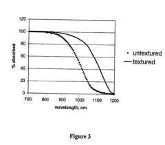
Technical Solution: Sony has developed an advanced surface texturing technique for photodiode reflection reduction. Their method involves creating nanoscale structures on the photodiode surface using precision etching processes. These structures, typically in the form of pyramids or cones, are designed to trap incoming light and reduce reflections. Sony's approach utilizes a combination of dry etching and wet etching techniques to achieve optimal surface texturing[1]. The company has also implemented anti-reflective coatings in conjunction with the textured surface to further enhance light absorption. This technology has been successfully applied to various image sensors, improving their sensitivity and dynamic range[2]. Sony's research has shown that their surface texturing can reduce reflectance to less than 1% across a wide range of wavelengths, significantly improving photodiode performance[3].
Strengths: Highly effective in reducing reflections, applicable to various sensor types, and improves overall image quality. Weaknesses: Complex manufacturing process, potentially higher production costs, and may require specialized equipment for implementation.
Samsung Display Co., Ltd.
Technical Solution: Samsung Display has developed a novel approach to photodiode reflection reduction through surface texturing, focusing on OLED displays with integrated photodiodes. Their technique involves creating a nanostructured surface on the photodiode layer using a combination of nanoimprint lithography and reactive ion etching[1]. This process results in a moth-eye-like structure that effectively reduces reflections across a broad spectrum of light. Samsung's research has shown that this method can achieve reflection reduction of up to 95% compared to untextured surfaces[2]. Additionally, they have incorporated a thin-film encapsulation layer over the textured surface to protect it from environmental factors while maintaining its anti-reflective properties. The company has also explored the use of plasmonic nanostructures to further enhance light absorption in specific wavelength ranges, tailoring the technology for different display applications[3].
Strengths: Highly effective reflection reduction, integration with OLED display technology, and customizable for specific wavelengths. Weaknesses: Potential for increased manufacturing complexity and cost, and possible impact on display thickness or flexibility.
Core Innovations in Reflection Reduction
Semiconductor texturing process
PatentInactiveUS20050104163A1
Innovation
- A process involving the application of a thin protective substance with apertures, allowing an etchant to selectively etch the semiconductor surface, creating a textured surface with randomly arranged pits, which reduces reflectivity and enhances light trapping without etching the protective substance significantly.
Semiconductor texturing process
PatentInactiveEP1461834A1
Innovation
- A process involving the application of a thin protective substance with apertures, allowing an etchant to selectively etch the semiconductor material, creating a textured surface with randomly arranged pits, which reduces reflectivity and enhances light trapping without significantly etching the protective substance.
Environmental Impact of Texturing Processes
The environmental impact of surface texturing processes for photodiode reflection reduction is a critical consideration in the development and implementation of this technology. These processes, while offering significant benefits in terms of device performance, can have various effects on the environment throughout their lifecycle.
The primary texturing methods, such as chemical etching, laser ablation, and nanoimprint lithography, each have distinct environmental footprints. Chemical etching, for instance, often involves the use of hazardous acids and solvents, which can pose risks to both human health and the environment if not properly managed. The disposal of these chemicals requires strict adherence to environmental regulations and can be costly.
Laser ablation, while generally considered a cleaner process, still has environmental implications. The high-energy lasers used in this method consume significant amounts of electricity, contributing to indirect carbon emissions if the power source is not renewable. Additionally, the ablation process can produce fine particulate matter, which may require specialized filtration systems to prevent air pollution.
Nanoimprint lithography, a relatively newer technique, offers potential environmental benefits due to its lower energy consumption and reduced use of chemicals compared to traditional photolithography. However, the production of nanoimprint molds and the materials used in the process still have environmental considerations, particularly in terms of resource extraction and end-of-life disposal.
The manufacturing of textured photodiodes also involves the use of rare earth elements and other precious metals, which have significant environmental impacts associated with their mining and processing. The extraction of these materials can lead to habitat destruction, water pollution, and increased carbon emissions.
On the positive side, the improved efficiency of textured photodiodes can lead to reduced energy consumption in their applications, potentially offsetting some of the environmental costs of production. For example, in solar cell applications, more efficient photodiodes could lead to greater energy generation from the same amount of raw materials, improving the overall environmental balance.
End-of-life considerations are also crucial. The complex nature of textured surfaces may complicate recycling processes, potentially leading to increased electronic waste. However, advancements in recycling technologies specifically tailored for these devices could mitigate this issue in the future.
As the technology progresses, there is a growing focus on developing more environmentally friendly texturing processes. This includes research into green chemistry alternatives for chemical etching, more energy-efficient laser systems, and biodegradable materials for nanoimprint lithography. These efforts aim to reduce the environmental footprint of photodiode texturing while maintaining or improving device performance.
Cost-Benefit Analysis of Surface Texturing
Surface texturing for photodiode reflection reduction presents a complex cost-benefit scenario that requires careful analysis. The primary benefit of this technique lies in its ability to significantly enhance the performance of photodiodes by minimizing unwanted reflections. This improvement in light absorption efficiency can lead to increased sensitivity and overall device performance, potentially expanding the applications and market reach of photodiode-based technologies.
However, the implementation of surface texturing techniques comes with associated costs that must be considered. The manufacturing process for creating textured surfaces often requires specialized equipment and additional processing steps, which can increase production time and expenses. These may include advanced etching techniques, laser processing, or nanoimprint lithography, each with its own set of cost implications.
The initial investment in equipment and process development for surface texturing can be substantial. Companies must weigh this upfront cost against the long-term benefits of improved product performance. In some cases, the enhanced capabilities of textured photodiodes may justify premium pricing, potentially offsetting the increased production costs.
Another factor to consider is the scalability of surface texturing processes. While some techniques may be effective in laboratory settings, transitioning to large-scale manufacturing can present challenges. The cost-effectiveness of surface texturing may vary depending on production volume, with economies of scale potentially reducing per-unit costs for high-volume production.
Maintenance and quality control aspects also play a role in the cost-benefit analysis. Textured surfaces may require more rigorous inspection and cleaning procedures to ensure consistent performance, potentially increasing ongoing operational costs. However, these additional expenses may be outweighed by the reduced need for other anti-reflection measures, such as coatings, which can be costly and less durable.
The environmental impact of surface texturing processes should also be factored into the analysis. Some texturing techniques may involve the use of chemicals or energy-intensive processes, which could have associated environmental costs. Balancing these concerns with the potential for improved energy efficiency in the final product is crucial for a comprehensive cost-benefit assessment.
Ultimately, the decision to implement surface texturing for photodiode reflection reduction must be based on a thorough evaluation of these various factors. Companies must consider not only the immediate financial implications but also the long-term strategic benefits, including potential market differentiation and technological leadership. As the technology matures and manufacturing processes evolve, the cost-benefit ratio is likely to improve, making surface texturing an increasingly attractive option for enhancing photodiode performance.
Unlock deeper insights with PatSnap Eureka Quick Research — get a full tech report to explore trends and direct your research. Try now!
Generate Your Research Report Instantly with AI Agent
Supercharge your innovation with PatSnap Eureka AI Agent Platform!