Effects of ionizing radiation on photodiode components
AUG 21, 20259 MIN READ
Generate Your Research Report Instantly with AI Agent
Patsnap Eureka helps you evaluate technical feasibility & market potential.
Radiation Effects on Photodiodes: Background and Objectives
Photodiodes have been integral components in various electronic and optical systems for decades, playing crucial roles in applications ranging from telecommunications to medical imaging. However, the effects of ionizing radiation on these semiconductor devices have become an increasingly important area of study, particularly as photodiodes find applications in harsh radiation environments such as space exploration, nuclear power plants, and high-energy physics experiments.
The evolution of photodiode technology has been marked by continuous improvements in sensitivity, response time, and reliability. From early silicon-based devices to advanced compound semiconductor photodiodes, the field has seen significant advancements. Concurrently, the understanding of radiation effects on these devices has grown, driven by the need for radiation-hardened components in critical applications.
Ionizing radiation, which includes gamma rays, X-rays, and high-energy particles, can cause both transient and permanent damage to photodiode components. These effects can manifest as increased dark current, reduced quantum efficiency, and altered spectral response characteristics. The severity and nature of these effects depend on factors such as radiation type, dose rate, total dose, and the specific materials and design of the photodiode.
The primary objective of studying radiation effects on photodiodes is to develop more resilient devices capable of maintaining their performance in radiation-rich environments. This involves understanding the fundamental mechanisms of radiation damage at the atomic and device levels, as well as exploring novel materials and device architectures that exhibit enhanced radiation tolerance.
Another key goal is to establish accurate models for predicting the long-term behavior of photodiodes under various radiation conditions. Such models are essential for designing systems with appropriate radiation shielding and for estimating the operational lifespan of devices in specific applications. This predictive capability is particularly crucial for space-based systems where in-situ repairs or replacements are often impossible.
Furthermore, research in this field aims to develop innovative techniques for mitigating radiation effects, such as annealing processes to reverse certain types of radiation damage or implementing redundancy and error-correction mechanisms at the system level. The ultimate aim is to push the boundaries of photodiode performance and reliability in extreme environments, enabling new applications and improving existing ones.
As technology continues to advance, there is a growing trend towards miniaturization and integration of photodiode-based systems. This trend introduces new challenges in radiation hardening, as smaller devices may be more susceptible to certain types of radiation damage. Consequently, the field is evolving to address these emerging issues while continuing to improve upon traditional radiation hardening techniques.
Market Analysis for Radiation-Hardened Photodiodes
The market for radiation-hardened photodiodes has been experiencing steady growth due to increasing demand in aerospace, nuclear power, and high-energy physics applications. These specialized components are crucial in environments where ionizing radiation can severely impact the performance and reliability of standard photodiodes. The global market for radiation-hardened electronics, including photodiodes, is projected to expand significantly over the next decade.
Key drivers of market growth include the burgeoning space industry, with a surge in satellite launches and deep space exploration missions. The commercial space sector, in particular, has been a major contributor to this growth, with companies like SpaceX, Blue Origin, and OneWeb deploying large satellite constellations. These projects require radiation-hardened components to ensure long-term operational reliability in the harsh space environment.
The nuclear power industry also represents a substantial market for radiation-hardened photodiodes. As countries worldwide invest in nuclear energy as a low-carbon power source, the demand for robust sensing and monitoring equipment capable of withstanding high radiation levels continues to rise. This trend is particularly evident in emerging economies expanding their nuclear power capabilities.
In the field of high-energy physics, large-scale research facilities such as particle accelerators and fusion reactors rely heavily on radiation-hardened photodiodes for various sensing and detection applications. The ongoing development of next-generation facilities and upgrades to existing ones contribute to the sustained demand in this sector.
The defense and military sector is another significant market for radiation-hardened photodiodes. These components are essential in missile guidance systems, satellite communications, and other mission-critical applications where radiation resistance is paramount. Increasing global defense spending and modernization efforts in many countries are driving growth in this segment.
Geographically, North America and Europe currently dominate the market for radiation-hardened photodiodes, owing to their advanced aerospace and defense industries. However, the Asia-Pacific region is expected to witness the fastest growth rate in the coming years, fueled by increasing investments in space programs and nuclear power plants in countries like China and India.
Despite the positive growth outlook, the market faces challenges such as high development and production costs, long qualification cycles, and stringent regulatory requirements. These factors can limit market entry for new players and slow down innovation cycles. Nevertheless, ongoing research into novel materials and manufacturing techniques holds promise for overcoming these obstacles and further expanding the market for radiation-hardened photodiodes.
Current Challenges in Radiation-Resistant Photodiode Design
The design of radiation-resistant photodiodes faces several significant challenges in the current technological landscape. One of the primary issues is the degradation of semiconductor materials when exposed to ionizing radiation. This exposure can lead to the creation of defects in the crystal structure, altering the electrical properties of the device and potentially causing permanent damage.
Another major challenge lies in maintaining the sensitivity and responsivity of photodiodes in high-radiation environments. Ionizing radiation can induce noise and increase dark current, which significantly impacts the signal-to-noise ratio and overall performance of the device. Engineers must develop innovative strategies to mitigate these effects without compromising the photodiode's primary function.
The trade-off between radiation hardness and device performance presents a complex optimization problem. Techniques that enhance radiation resistance, such as using thicker oxide layers or specialized doping profiles, often come at the cost of reduced quantum efficiency or increased response time. Balancing these competing factors requires careful design considerations and advanced modeling techniques.
Thermal management is another critical challenge in radiation-resistant photodiode design. Radiation-induced heating can exacerbate existing issues and introduce new failure modes. Developing effective heat dissipation mechanisms that do not interfere with the device's optical properties is crucial for long-term reliability in high-radiation environments.
The miniaturization trend in electronics poses additional challenges for radiation-hardened photodiodes. As devices become smaller, they become more susceptible to single-event effects caused by individual particles. Designing compact yet robust structures that can withstand these effects without compromising functionality is an ongoing area of research.
Material selection and development represent another frontier in addressing current challenges. While traditional silicon-based photodiodes have been widely used, there is growing interest in alternative materials such as silicon carbide, gallium nitride, and diamond for their potential radiation-resistant properties. However, integrating these materials into existing manufacturing processes and ensuring their long-term stability under radiation exposure remain significant hurdles.
Lastly, the development of accurate and reliable testing methodologies for radiation-resistant photodiodes is a persistent challenge. Simulating real-world radiation environments and accelerated aging tests that can predict long-term performance are essential for validating design improvements. Creating standardized testing protocols that can be universally applied across different photodiode designs and applications is an ongoing effort in the industry.
Existing Radiation Mitigation Strategies for Photodiodes
01 Photodiode structure and materials
Photodiodes are typically constructed using semiconductor materials such as silicon or germanium. The structure often includes a p-n junction or PIN (p-type, intrinsic, n-type) configuration. The choice of materials and structure affects the photodiode's sensitivity, response time, and spectral range.- Photodiode structure and materials: Photodiodes are constructed using various semiconductor materials and structures to optimize their performance. This includes the use of different layers, doping profiles, and materials such as silicon, germanium, or III-V compounds. The structure and materials chosen affect the photodiode's sensitivity, response time, and spectral range.
- Integration with other components: Photodiodes are often integrated with other electronic components to create more complex devices. This integration can include amplifiers, readout circuits, or other optical elements. Such integration can improve overall system performance, reduce noise, and enable advanced functionalities in applications like imaging sensors or optical communication devices.
- Wavelength sensitivity and spectral response: The spectral response of photodiodes can be tailored to specific wavelengths or ranges of light. This is achieved through careful selection of materials, the use of optical filters, or specialized structures like quantum wells. Enhancing sensitivity to specific wavelengths is crucial for applications in spectroscopy, color sensing, and infrared detection.
- Noise reduction and signal enhancement: Various techniques are employed to reduce noise and enhance the signal in photodiode-based systems. This can include the use of cooling systems, specialized readout circuits, or signal processing algorithms. Improving the signal-to-noise ratio is essential for achieving high sensitivity and accuracy in applications such as low-light imaging or precise optical measurements.
- Packaging and environmental protection: The packaging of photodiodes plays a crucial role in their performance and reliability. Proper packaging can protect the device from environmental factors such as moisture, temperature fluctuations, and mechanical stress. Additionally, specialized packaging techniques can enhance optical coupling, improve thermal management, or enable integration into specific form factors for various applications.
02 Light detection and conversion
Photodiodes convert light into electrical current through the photovoltaic effect. The efficiency of this conversion depends on factors such as the incident light wavelength, the photodiode's active area, and the semiconductor material's bandgap. Improvements in light detection and conversion can enhance the overall performance of devices using photodiodes.Expand Specific Solutions03 Integration with other components
Photodiodes are often integrated with other electronic components to form more complex devices. This integration can include amplifiers, readout circuits, or other signal processing elements. The design of these integrated systems affects the overall performance, power consumption, and functionality of the device.Expand Specific Solutions04 Noise reduction and sensitivity improvement
Enhancing the sensitivity of photodiodes while reducing noise is crucial for many applications. Techniques such as cooling, optimizing the device geometry, and using advanced materials can help improve the signal-to-noise ratio and overall sensitivity of photodiodes.Expand Specific Solutions05 Application-specific designs
Photodiodes are used in various applications, including optical communication, imaging sensors, and scientific instruments. Each application may require specific design considerations, such as high-speed response for communications or large-area detectors for imaging. Tailoring the photodiode design to the specific application can significantly improve overall system performance.Expand Specific Solutions
Key Players in Radiation-Hardened Photodiode Industry
The effects of ionizing radiation on photodiode components represent a critical area of research in the semiconductor industry, currently in a mature development stage. The market for radiation-hardened photodiodes is growing steadily, driven by applications in aerospace, nuclear energy, and medical imaging. Companies like Honeywell International Technologies, DB HITEK, and Sony Semiconductor Solutions are at the forefront of developing radiation-resistant photodiodes. Research institutions such as the Harbin Institute of Technology and the Commissariat à l'énergie atomique et aux énergies Alternatives are contributing significantly to advancing the understanding of radiation effects on semiconductor devices. The technology's maturity is evident in the commercial availability of radiation-hardened photodiodes, but ongoing research continues to improve their performance and reliability in high-radiation environments.
Honeywell International Technologies Ltd.
Technical Solution: Honeywell has developed radiation-hardened photodiodes using a combination of advanced materials and innovative design techniques. Their approach involves the use of III-V compound semiconductors, particularly gallium arsenide (GaAs) and indium gallium arsenide (InGaAs), which offer inherently higher radiation resistance compared to silicon[1]. Honeywell's photodiodes feature a multi-layer epitaxial structure with carefully engineered doping profiles to optimize charge collection and minimize radiation-induced defects. They have also implemented specialized surface passivation techniques and anti-reflection coatings to enhance device stability and quantum efficiency under radiation exposure[3]. Additionally, Honeywell has developed proprietary packaging solutions that provide additional shielding against high-energy particles, further improving the overall radiation hardness of their photodiode components[5].
Strengths: High radiation resistance, excellent performance in harsh environments, and proven track record in aerospace and defense applications. Weaknesses: Higher production costs due to specialized materials and processes, and potential limitations in integration with standard silicon-based electronics.
OSRAM Opto Semiconductors GmbH
Technical Solution: OSRAM Opto Semiconductors has developed radiation-resistant photodiodes using advanced semiconductor materials and innovative device architectures. Their approach focuses on the use of wide-bandgap materials such as silicon carbide (SiC) and gallium nitride (GaN) to create photodiodes with inherently higher radiation tolerance[2]. OSRAM's devices feature a unique heterostructure design that incorporates multiple quantum wells to enhance light absorption and carrier collection efficiency. They have also implemented specialized doping techniques and surface treatments to minimize radiation-induced defects and improve long-term stability[4]. Additionally, OSRAM has developed proprietary packaging solutions that provide enhanced thermal management and protection against environmental factors, further improving the overall reliability of their photodiodes in high-radiation environments[6].
Strengths: High radiation resistance, excellent performance in extreme conditions, and potential for integration with other optoelectronic components. Weaknesses: Higher manufacturing costs compared to traditional photodiodes, and potential challenges in achieving high responsivity across a broad spectral range.
Core Innovations in Radiation-Resistant Photodiode Technology
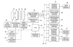
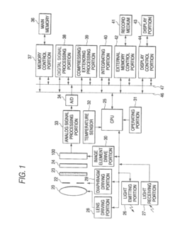
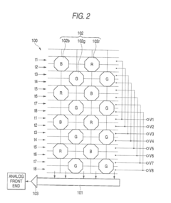
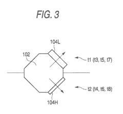
Semiconductor element, method of driving semiconductor element and solid imaging apparatus
PatentInactiveUS20080088723A1
Innovation
- The semiconductor element employs multiple read gates with varying amplification factors positioned strategically relative to photoelectric conversion portions and vertical transfer paths, allowing for tailored signal charge amplification to suit imaging conditions, thereby reducing noise and maintaining consistent image quality.
Radiation Testing and Qualification Standards
Radiation testing and qualification standards play a crucial role in ensuring the reliability and performance of photodiode components exposed to ionizing radiation. These standards provide a framework for evaluating the effects of radiation on electronic devices and establishing their suitability for use in radiation-intensive environments.
The primary standards governing radiation testing for photodiodes include MIL-STD-883, Method 1019 for ionizing radiation testing, and ASTM F1892 for proton radiation testing. These standards outline specific procedures for exposing devices to controlled doses of radiation and measuring their subsequent performance characteristics.
MIL-STD-883, Method 1019 focuses on total ionizing dose (TID) effects and specifies test conditions, radiation sources, and measurement techniques. It typically involves exposing photodiodes to gamma radiation from a Cobalt-60 source at various dose rates and total doses. The standard requires monitoring key parameters such as dark current, responsivity, and spectral response before, during, and after irradiation.
ASTM F1892 addresses the effects of proton radiation, which is particularly relevant for space applications. This standard outlines procedures for exposing photodiodes to high-energy protons and evaluating their impact on device performance. It includes guidelines for proton energy selection, fluence levels, and post-irradiation characterization.
In addition to these primary standards, the European Space Agency (ESA) has developed ESCC Basic Specification No. 22900, which provides comprehensive guidelines for radiation hardness assurance and testing of optoelectronic devices, including photodiodes. This specification covers both TID and displacement damage effects.
Qualification standards often require accelerated testing to simulate long-term radiation exposure in a shorter timeframe. This approach involves exposing devices to higher radiation doses than they would typically encounter in their intended application, allowing for the assessment of cumulative damage effects.
To meet these standards, photodiode manufacturers and users must implement rigorous testing protocols. This includes pre-irradiation characterization, in-situ measurements during radiation exposure, and post-irradiation analysis. The testing process often involves specialized equipment such as radiation sources, dosimetry systems, and precision measurement instruments.
Compliance with these standards is essential for qualifying photodiodes for use in radiation-intensive applications, such as space exploration, nuclear power plants, and high-energy physics experiments. The qualification process helps identify radiation-tolerant designs and materials, enabling the development of more robust photodiode components for these challenging environments.
Environmental Impact of Radiation-Hardened Materials
The environmental impact of radiation-hardened materials used in photodiode components is a critical consideration in the development and deployment of these devices. These materials, designed to withstand ionizing radiation, often contain elements and compounds that can pose significant environmental risks if not properly managed throughout their lifecycle.
Radiation-hardened materials typically include specialized semiconductors, insulators, and packaging materials. Many of these components incorporate rare earth elements, heavy metals, and complex synthetic compounds. While these materials are essential for ensuring the reliability of photodiodes in high-radiation environments, their production, use, and disposal can have far-reaching environmental consequences.
The manufacturing process of radiation-hardened materials often involves energy-intensive techniques and the use of hazardous chemicals. This can lead to increased carbon emissions and the potential release of toxic substances into the environment. Additionally, the extraction of rare earth elements and other raw materials required for these components can result in habitat destruction, soil erosion, and water pollution in mining areas.
During the operational life of radiation-hardened photodiodes, the environmental impact is generally minimal. However, the disposal of these components at the end of their lifecycle presents significant challenges. Improper disposal can lead to the leaching of harmful substances into soil and groundwater, potentially contaminating ecosystems and posing risks to human health.
Recycling radiation-hardened materials is complex due to their specialized composition. The process often requires advanced separation techniques and can be energy-intensive. However, effective recycling programs can help mitigate environmental impacts by reducing the need for new raw material extraction and minimizing waste.
To address these environmental concerns, researchers and manufacturers are exploring more sustainable alternatives. This includes developing radiation-hardening techniques that rely on less environmentally harmful materials and improving the recyclability of components. Additionally, there is a growing focus on designing photodiodes with longer operational lifespans, reducing the frequency of replacement and disposal.
Regulatory bodies are also playing a crucial role in mitigating the environmental impact of radiation-hardened materials. Stricter guidelines for manufacturing processes, material selection, and end-of-life management are being implemented in many countries. These regulations aim to promote more sustainable practices throughout the lifecycle of radiation-hardened photodiode components.
Unlock deeper insights with Patsnap Eureka Quick Research — get a full tech report to explore trends and direct your research. Try now!
Generate Your Research Report Instantly with AI Agent
Supercharge your innovation with Patsnap Eureka AI Agent Platform!