Innovation trends in transparent photodiode displays
AUG 21, 20259 MIN READ
Generate Your Research Report Instantly with AI Agent
Patsnap Eureka helps you evaluate technical feasibility & market potential.
Display Tech Evolution
The evolution of display technology has been marked by significant advancements over the past few decades, with transparent photodiode displays emerging as a promising frontier. This technological progression can be traced back to the early cathode ray tubes (CRTs) of the mid-20th century, which laid the foundation for electronic visual displays.
The transition from CRTs to liquid crystal displays (LCDs) in the 1970s and 1980s represented a major leap forward, offering thinner, more energy-efficient screens. This was followed by the development of plasma display panels (PDPs) in the 1990s, which provided improved contrast and viewing angles for larger screens.
The early 2000s saw the rise of organic light-emitting diode (OLED) technology, which revolutionized display quality with its ability to produce deep blacks and vibrant colors. OLED displays also paved the way for flexible and transparent screen concepts, setting the stage for innovations in transparent photodiode displays.
Transparent displays began to gain traction in the 2010s, with various prototypes demonstrating the potential for see-through screens. These early iterations often relied on projection systems or specialized LCD configurations. However, the integration of photodiodes into transparent displays marks a significant evolution in this field.
Photodiode-based transparent displays leverage the unique properties of certain semiconductor materials that can both detect light and generate electrical signals. This dual functionality allows for the creation of displays that can not only present visual information but also capture ambient light or even images, opening up new possibilities for interactive and context-aware screens.
Recent years have seen accelerated research and development in transparent photodiode displays, with improvements in transparency levels, resolution, and response times. The use of novel materials such as indium gallium zinc oxide (IGZO) and amorphous silicon has contributed to enhanced performance and manufacturability.
The ongoing miniaturization of photodiode components and advancements in thin-film transistor (TFT) technology have further propelled the field forward. These developments have enabled the creation of displays with higher pixel densities and improved light sensitivity, crucial factors for the practical implementation of transparent photodiode displays in various applications.
As we look to the future, the trajectory of transparent photodiode displays points towards increased integration with augmented reality (AR) and smart surface technologies. The potential for these displays to seamlessly blend digital information with the physical environment presents exciting possibilities for sectors ranging from automotive head-up displays to smart windows in architecture and interactive retail experiences.
Market Demand Analysis
The market demand for transparent photodiode displays has been steadily increasing in recent years, driven by the growing need for innovative display technologies across various industries. This emerging technology offers unique advantages over traditional displays, combining transparency with light-sensing capabilities, which opens up new possibilities for interactive and energy-efficient display applications.
In the consumer electronics sector, there is a rising demand for transparent displays in smartphones, smartwatches, and augmented reality (AR) devices. These displays enable seamless integration of digital information with the real world, enhancing user experience and functionality. The automotive industry has also shown significant interest in transparent photodiode displays for heads-up displays (HUDs) and smart windshields, improving driver safety and providing real-time information without obstructing the view.
The retail and advertising sectors are exploring the potential of transparent photodiode displays for interactive storefronts and digital signage. These displays offer a novel way to engage customers and create immersive shopping experiences. Additionally, the architecture and interior design industries are increasingly incorporating transparent displays into smart windows and glass partitions, allowing for dynamic control of light and privacy while doubling as information displays.
In the healthcare sector, transparent photodiode displays are being considered for medical imaging applications and smart hospital room dividers. These displays can provide real-time patient information while maintaining visibility and light transmission. The aerospace industry is also showing interest in this technology for cockpit displays and passenger cabin windows, enhancing both functionality and passenger experience.
The market for transparent photodiode displays is expected to grow significantly in the coming years. Factors driving this growth include advancements in material science, increasing adoption of IoT and smart devices, and the growing demand for energy-efficient display solutions. However, challenges such as production costs, durability, and scalability need to be addressed to fully realize the market potential.
As the technology matures and production costs decrease, we can expect to see wider adoption across various industries. The ability of transparent photodiode displays to seamlessly blend digital information with the physical environment positions them as a key enabling technology for future smart cities, connected vehicles, and immersive AR experiences. This convergence of display and sensing technologies is likely to create new market opportunities and drive innovation in user interfaces and interaction paradigms.
Current Challenges
Transparent photodiode displays represent a cutting-edge technology with immense potential, yet they face several significant challenges that hinder their widespread adoption and commercialization. One of the primary obstacles is the trade-off between transparency and performance. As the transparency of the display increases, the efficiency of light absorption and conversion typically decreases, leading to reduced sensitivity and overall performance of the photodiodes.
Another major challenge lies in the materials used for transparent photodiodes. Current materials often struggle to achieve the desired balance of transparency, conductivity, and photoelectric conversion efficiency. Many transparent conducting oxides (TCOs) used in these displays exhibit limited charge carrier mobility, which can negatively impact the response time and sensitivity of the photodiodes.
The fabrication process for transparent photodiode displays presents its own set of difficulties. Achieving uniform deposition of transparent conductive layers over large areas while maintaining consistent performance across the entire display remains a significant technical hurdle. Additionally, the integration of transparent photodiodes with existing display technologies, such as OLEDs or LCDs, poses challenges in terms of compatibility and manufacturing complexity.
Stability and durability of transparent photodiode displays are also areas of concern. Many of the materials used are susceptible to degradation when exposed to environmental factors such as moisture, oxygen, and UV radiation. This can lead to reduced lifespan and reliability of the displays, particularly in outdoor or harsh environments.
The cost of production remains a significant barrier to widespread adoption. The specialized materials and complex fabrication processes required for transparent photodiode displays result in higher manufacturing costs compared to conventional display technologies. This cost factor limits their competitiveness in the consumer electronics market and slows down their integration into mainstream devices.
Furthermore, the development of efficient and transparent color filters for these displays presents another challenge. Achieving high color purity and contrast while maintaining transparency is a delicate balance that researchers are still working to optimize.
Lastly, the challenge of power consumption in transparent photodiode displays cannot be overlooked. While these displays have the potential to be energy-efficient, optimizing their power usage while maintaining high performance and transparency remains an ongoing area of research and development.
Existing Solutions
01 Transparent photodiode structure
Transparent photodiodes are designed with specific structures to achieve high transparency while maintaining photodetection capabilities. These structures may include the use of transparent conductive materials, thin-film designs, and optimized layer configurations to allow light transmission while efficiently capturing photons for electrical conversion.- Transparent photodiode structure: Transparent photodiodes are designed with specific structures to achieve transparency while maintaining their light-sensing capabilities. These structures may include the use of transparent conductive materials, thin-film designs, and specialized electrode configurations to allow light to pass through while still detecting it.
- Integration with display technologies: Transparent photodiodes can be integrated with various display technologies to create transparent displays with light-sensing capabilities. This integration may involve incorporating photodiodes into OLED, LCD, or other display types, enabling features such as ambient light sensing or touch detection without compromising display transparency.
- Materials for transparent photodiodes: The choice of materials is crucial for creating transparent photodiodes. Researchers explore various materials such as transparent conductive oxides, graphene, and other novel materials to achieve high transparency and efficient light detection simultaneously.
- Transparency enhancement techniques: Various techniques are employed to enhance the transparency of photodiode displays. These may include optimizing layer thicknesses, using anti-reflection coatings, and developing novel fabrication methods to minimize light absorption and scattering within the device structure.
- Applications of transparent photodiode displays: Transparent photodiode displays find applications in various fields, including augmented reality, heads-up displays, smart windows, and wearable devices. These applications leverage the unique combination of transparency and light-sensing capabilities to create innovative user interfaces and interactive environments.
02 Integration with display technologies
Transparent photodiodes can be integrated with various display technologies to create transparent displays with sensing capabilities. This integration may involve incorporating photodiodes into pixel structures, using them as part of touch-sensing layers, or combining them with transparent OLED or LCD panels to create multi-functional display devices.Expand Specific Solutions03 Transparent conductive materials
The use of transparent conductive materials is crucial for creating transparent photodiode displays. Materials such as indium tin oxide (ITO), graphene, or conductive polymers are employed to form electrodes and interconnects that allow light transmission while maintaining electrical conductivity, enabling the fabrication of transparent electronic components.Expand Specific Solutions04 Optical design for transparency enhancement
Various optical design techniques are employed to enhance the transparency of photodiode displays. These may include anti-reflection coatings, micro-lens arrays, or specialized light management structures that minimize light absorption and scattering, thereby improving overall transparency and display performance.Expand Specific Solutions05 Transparent display applications
Transparent photodiode displays find applications in various fields, including augmented reality (AR) devices, heads-up displays, smart windows, and transparent electronic devices. These applications leverage the combination of transparency and sensing capabilities to create innovative user interfaces and interactive experiences.Expand Specific Solutions
Key Industry Players
The innovation landscape for transparent photodiode displays is in an early growth stage, characterized by rapid technological advancements and increasing market potential. The global market size for this technology is expanding, driven by applications in consumer electronics, automotive displays, and smart windows. While still emerging, the technology is progressing towards commercial viability. Key players like LG Display, BOE Technology, and Samsung Display are investing heavily in R&D to overcome challenges in transparency and efficiency. Smaller companies such as Ubiquitous Energy are also making significant strides, particularly in niche applications. The competitive landscape is dynamic, with both established display manufacturers and innovative startups vying for market share and technological breakthroughs.
LG Display Co., Ltd.
Technical Solution: LG Display has been pioneering transparent OLED technology for photodiode displays. Their innovative approach involves integrating transparent OLED panels with photodiodes to create displays that can both emit and detect light. This technology allows for touch-free gesture control and ambient light sensing capabilities[1]. LG's transparent OLED displays achieve up to 40% transparency, significantly higher than conventional LCDs[2]. They have also developed a 55-inch transparent OLED display with a contrast ratio of 150,000:1 and a wide color gamut covering 120% of the DCI-P3 color space[3].
Strengths: High transparency, excellent image quality, and innovative touch-free control. Weaknesses: Higher production costs compared to traditional displays and limited mass production capabilities.
BOE Technology Group Co., Ltd.
Technical Solution: BOE has made significant strides in transparent photodiode display technology, focusing on a-Si TFT backplane with integrated photodiodes. Their approach involves embedding photodiodes within each pixel of the display, allowing for both light emission and detection[4]. BOE's transparent displays achieve a transparency of up to 50% while maintaining a resolution of 1920x1080[5]. They have also developed a 55-inch transparent LCD with a response time of 8ms and a brightness of 500 nits[6]. BOE's technology enables touch-free interaction and ambient light sensing, making it suitable for various applications including automotive HUDs and smart home devices.
Strengths: High transparency, good resolution, and versatile applications. Weaknesses: Lower contrast ratio compared to OLED technology and potential issues with uniformity in large displays.
Core Innovations
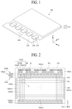
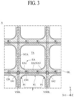
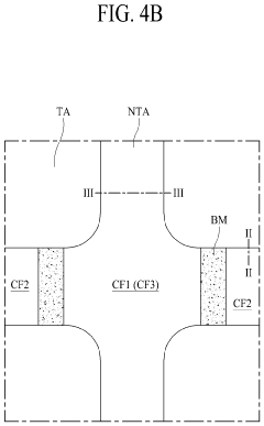
Transparent display device having display area including transmissive area and non-transmissive area
PatentActiveUS11950459B2
Innovation
- The design includes a substrate with a display area divided into transmissive and non-transmissive areas, featuring insulating layers and anode electrodes with specific protrusions to cover metal lines, and the removal of high refractive index layers and banks from the transmissive area to enhance light transmittance and prevent yellowish phenomena.
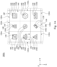
Micro light-emitting diode transparent display
PatentActiveUS20210035958A1
Innovation
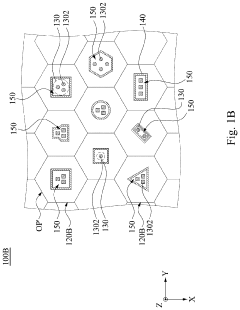
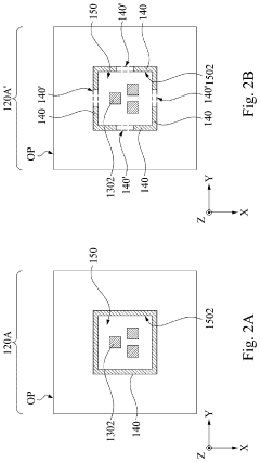
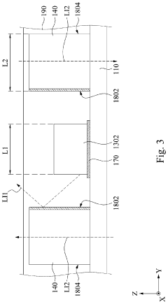
- A micro light-emitting diode transparent display is designed with a transparent substrate, N pixels, and N sets of micro light-emitting diodes, where a wall portion surrounds each set of diodes to form an enclosed region with a periphery length equal to or less than 85% of the pixel's outer periphery, allowing light to pass through and increasing transparency.
Material Advancements
Transparent photodiode displays have seen significant advancements in materials science, driving innovation and improving performance. The development of novel materials has been crucial in enhancing transparency, sensitivity, and overall efficiency of these displays.
One of the key areas of material advancement is in the development of transparent conducting electrodes. Traditional indium tin oxide (ITO) has been widely used, but researchers are exploring alternatives to overcome its limitations. Graphene, a single layer of carbon atoms, has emerged as a promising candidate due to its high conductivity and transparency. Recent studies have shown that graphene-based electrodes can achieve over 90% transparency while maintaining excellent electrical properties.
Another important material innovation is in the active layer of photodiodes. Organic semiconductors have gained attention for their flexibility and potential for large-area fabrication. Researchers have developed new organic compounds with improved light absorption and charge transport properties. For instance, novel donor-acceptor copolymers have been synthesized, demonstrating enhanced photosensitivity across a broader spectrum of light.
Quantum dots have also made significant contributions to material advancements in transparent photodiode displays. These nanoscale semiconductor particles offer tunable optical properties and high quantum efficiency. Recent developments in quantum dot synthesis have led to materials with improved stability and reduced toxicity, making them more suitable for commercial applications.
Perovskite materials have shown great promise in photodiode technology. Their unique crystal structure allows for efficient light absorption and charge separation. Researchers have made progress in developing lead-free perovskites, addressing environmental concerns while maintaining high performance. These materials have demonstrated remarkable photosensitivity and can be processed at low temperatures, enabling integration with flexible substrates.
Advancements in nanostructured materials have also played a crucial role. Nanowires and nanoparticles have been incorporated into photodiode structures to enhance light trapping and increase sensitivity. For example, zinc oxide nanowires have been used to create highly transparent and sensitive UV photodetectors.
The development of hybrid materials, combining organic and inorganic components, has opened new possibilities for transparent photodiode displays. These materials leverage the advantages of both classes, resulting in improved stability, efficiency, and ease of processing. Recent research has focused on optimizing the interface between organic and inorganic layers to enhance charge transfer and reduce recombination losses.
These material advancements have collectively contributed to pushing the boundaries of transparent photodiode display technology, enabling higher transparency, improved sensitivity, and enhanced overall performance. As research in materials science continues to progress, we can expect further innovations that will drive the development of next-generation transparent photodiode displays.
Energy Efficiency
Energy efficiency is a critical aspect of transparent photodiode displays, driving innovation trends in this emerging technology. As these displays gain traction in various applications, from smart windows to augmented reality devices, the need for power-efficient solutions becomes paramount. Recent advancements in materials science and device engineering have paved the way for significant improvements in energy consumption.
One of the primary focuses in energy efficiency for transparent photodiode displays is the development of low-power active layers. Researchers are exploring novel semiconductor materials that exhibit high charge carrier mobility and low off-state current. These properties allow for faster switching and reduced power consumption during operation. Additionally, the integration of wide-bandgap materials has shown promise in minimizing leakage currents, further enhancing overall energy efficiency.
Another area of innovation lies in the optimization of device architectures. Multi-junction structures and tandem configurations are being investigated to improve light absorption and charge collection efficiency. By carefully engineering the layer stack and incorporating light-trapping features, researchers aim to maximize the utilization of incident light, thereby reducing the power required for display operation.
Advanced power management techniques are also playing a crucial role in enhancing energy efficiency. Adaptive refresh rates and selective pixel activation strategies are being implemented to minimize unnecessary power consumption. These approaches allow the display to dynamically adjust its power usage based on the content being displayed and ambient lighting conditions.
The integration of energy harvesting capabilities is an emerging trend in transparent photodiode displays. By incorporating photovoltaic elements within the display structure, researchers are exploring ways to capture ambient light and convert it into usable energy. This self-powering feature has the potential to significantly reduce the overall energy footprint of devices utilizing these displays.
Improvements in manufacturing processes are contributing to energy efficiency gains as well. The development of low-temperature fabrication techniques enables the use of flexible and lightweight substrates, reducing the energy required for production. Additionally, advancements in large-area deposition methods are enhancing the uniformity and performance of transparent photodiode arrays, leading to more efficient and reliable displays.
As the field progresses, the focus on energy efficiency is expected to drive further innovations in materials, device architectures, and system-level optimizations. The convergence of these advancements will play a crucial role in realizing the full potential of transparent photodiode displays across various applications, from consumer electronics to smart infrastructure.
Unlock deeper insights with Patsnap Eureka Quick Research — get a full tech report to explore trends and direct your research. Try now!
Generate Your Research Report Instantly with AI Agent
Supercharge your innovation with Patsnap Eureka AI Agent Platform!
