

Photodiode design features influencing data throughput
AUG 21, 20259 MIN READ
Generate Your Research Report Instantly with AI Agent
PatSnap Eureka helps you evaluate technical feasibility & market potential.
Photodiode Throughput Evolution and Objectives
Photodiodes have undergone significant evolution since their inception, with a primary focus on enhancing data throughput capabilities. The journey began with simple PIN (Positive-Intrinsic-Negative) structures, which offered modest performance in terms of speed and sensitivity. As technology progressed, the demand for higher data rates in optical communication systems drove the development of more advanced photodiode designs.
The advent of avalanche photodiodes (APDs) marked a crucial milestone in this evolution. APDs introduced internal gain mechanisms, dramatically improving sensitivity and enabling the detection of weaker optical signals. This breakthrough allowed for longer transmission distances and higher data rates in fiber-optic networks. Concurrently, efforts were made to reduce the capacitance and increase the bandwidth of photodiodes, directly impacting their ability to handle higher data throughput.
In recent years, the focus has shifted towards integrating photodiodes with other optical and electronic components to create more compact and efficient optoelectronic systems. This integration has led to the development of photodiode arrays and monolithically integrated receivers, which can handle multiple channels simultaneously, further increasing overall data throughput.
The current technological landscape demands photodiodes capable of supporting data rates in the range of hundreds of gigabits per second. This requirement has spurred research into novel materials and structures, such as III-V compound semiconductors and nanoscale designs, to push the boundaries of photodiode performance.
Looking ahead, the objectives for photodiode design are multifaceted. Firstly, there is a continuous drive to increase bandwidth, aiming for terahertz-range operation to support future ultra-high-speed communication systems. Secondly, improving quantum efficiency across a broader spectrum of wavelengths is crucial for enhancing sensitivity and enabling more flexible optical network designs.
Another key objective is the reduction of dark current and noise, which are critical factors limiting the signal-to-noise ratio and, consequently, the achievable data rates. Additionally, there is a growing emphasis on developing photodiodes that can operate efficiently at room temperature, eliminating the need for costly cooling systems in high-performance applications.
Lastly, as the demand for miniaturization continues, a significant goal is to further integrate photodiodes with other optoelectronic components, creating more compact and energy-efficient systems. This integration aims to reduce overall system complexity and cost while maintaining or improving performance metrics crucial for high-throughput data transmission.
Market Demand for High-Speed Photodiodes
The market demand for high-speed photodiodes has been experiencing significant growth in recent years, driven by the increasing need for faster data transmission and processing across various industries. This surge in demand is primarily fueled by the rapid expansion of telecommunications networks, the proliferation of data centers, and the advancement of emerging technologies such as 5G, Internet of Things (IoT), and autonomous vehicles.
In the telecommunications sector, the deployment of fiber-optic networks and the ongoing transition to higher bandwidth systems have created a strong demand for high-speed photodiodes. These devices are crucial components in optical receivers, enabling the conversion of optical signals into electrical signals at high data rates. As network operators continue to upgrade their infrastructure to support increasing data traffic, the demand for photodiodes capable of handling higher frequencies and data throughput is expected to rise.
The data center industry has also become a significant driver of high-speed photodiode demand. With the exponential growth of cloud computing, big data analytics, and video streaming services, data centers require increasingly faster and more efficient optical communication systems. High-speed photodiodes play a vital role in these systems, facilitating rapid data transfer between servers and across long-distance networks.
Emerging technologies such as 5G and IoT are further amplifying the market demand for high-speed photodiodes. The rollout of 5G networks necessitates advanced optical components capable of supporting ultra-high-speed data transmission. Similarly, the expanding IoT ecosystem, with its vast network of interconnected devices, requires efficient and high-performance optical communication solutions.
The automotive industry is another sector contributing to the growing demand for high-speed photodiodes. As vehicles become more autonomous and connected, the need for advanced sensing and communication systems increases. High-speed photodiodes are essential components in LiDAR (Light Detection and Ranging) systems, which are crucial for autonomous vehicle navigation and obstacle detection.
Market analysts project that the global high-speed photodiode market will continue to expand at a compound annual growth rate (CAGR) of over 8% in the coming years. This growth is expected to be particularly strong in regions with rapidly developing digital infrastructure, such as Asia-Pacific and North America.
However, the market demand for high-speed photodiodes is not without challenges. The increasing complexity of optical systems and the need for higher performance often lead to higher costs, which can be a limiting factor for some applications. Additionally, the ongoing global semiconductor shortage has impacted the availability of components, potentially affecting the supply chain for high-speed photodiodes.
Despite these challenges, the overall market outlook for high-speed photodiodes remains positive. The continuous advancements in photodiode design and manufacturing processes are expected to address current limitations and open up new application areas, further driving market growth and innovation in this critical technology sector.
Current Challenges in Photodiode Data Throughput
Photodiodes face several significant challenges in achieving higher data throughput rates, which are crucial for advancing optical communication systems and sensor technologies. One of the primary obstacles is the inherent trade-off between speed and sensitivity. As the active area of a photodiode increases, its sensitivity improves, but at the cost of increased capacitance, which limits the device's speed and, consequently, its data throughput.
Another critical challenge is the management of dark current, which introduces noise and reduces the signal-to-noise ratio (SNR) of the photodiode. As manufacturers strive to enhance sensitivity, particularly in low-light conditions, controlling dark current becomes increasingly difficult. This issue is especially pronounced in avalanche photodiodes (APDs) and single-photon avalanche diodes (SPADs), where the high internal gain mechanism can amplify both signal and noise.
The bandwidth limitation of photodiodes also poses a significant hurdle in achieving higher data rates. The transit time of carriers through the depletion region and the RC time constant of the device structure both contribute to this limitation. As data rates increase, these factors become more pronounced, leading to inter-symbol interference and reduced eye diagram openings.
Thermal management is another pressing concern, particularly in high-power applications. As photodiodes handle higher optical powers and operate at faster speeds, heat dissipation becomes a critical factor. Excessive heat can lead to performance degradation, increased dark current, and even device failure, thus limiting the achievable data throughput.
The challenge of achieving uniform responsivity across a wide spectral range is also significant. Many applications require photodiodes to operate efficiently over broad wavelength ranges, but current designs often struggle to maintain consistent performance across the entire spectrum. This limitation can restrict the versatility and applicability of photodiodes in multi-wavelength communication systems.
Furthermore, the integration of photodiodes with readout circuits and other optical components presents its own set of challenges. As systems demand higher levels of integration for improved performance and reduced form factors, issues such as crosstalk, parasitic capacitances, and impedance matching become more pronounced, potentially limiting the overall system's data throughput capabilities.
Lastly, the manufacturing processes for high-performance photodiodes, especially those utilizing novel materials or structures, face scalability and cost challenges. Achieving consistent performance across large production volumes while maintaining economic viability is crucial for widespread adoption of advanced photodiode technologies in high-throughput applications.
Existing Solutions for Enhancing Data Throughput
01 High-speed data transmission in photodiode systems
Techniques for improving data throughput in photodiode-based systems, including optimized signal processing, advanced modulation schemes, and efficient data encoding methods. These approaches aim to maximize the amount of data that can be transmitted and received through photodiodes in a given time period.- High-speed data transmission in photodiode systems: Techniques for improving data throughput in photodiode-based systems, including optimized signal processing, advanced modulation schemes, and efficient data encoding methods. These approaches aim to maximize the amount of data that can be transmitted and received through photodiodes in a given time period.
- Parallel processing for increased photodiode data throughput: Implementation of parallel processing architectures to handle multiple data streams from photodiode arrays simultaneously. This approach allows for increased overall data throughput by distributing the processing load across multiple channels or processors.
- Optical networking and multiplexing for photodiode data: Utilization of optical networking techniques and multiplexing methods to enhance data throughput in photodiode-based communication systems. This includes wavelength division multiplexing (WDM) and other optical signal combining techniques to increase the overall data capacity of the system.
- Advanced signal processing for photodiode data: Implementation of sophisticated signal processing algorithms and techniques to improve the quality and speed of data extraction from photodiode outputs. This includes noise reduction, signal amplification, and advanced filtering methods to enhance the overall data throughput and reliability of photodiode-based systems.
- High-speed interface designs for photodiode data transfer: Development of specialized high-speed interfaces and bus architectures optimized for transferring data from photodiodes to processing units or storage systems. These designs focus on minimizing latency and maximizing bandwidth to achieve higher data throughput in photodiode applications.
02 Optical network optimization for photodiode data transfer
Methods for enhancing data throughput in optical networks utilizing photodiodes, focusing on network architecture improvements, traffic management, and bandwidth allocation strategies. These optimizations help to increase overall system efficiency and data transfer rates in photodiode-based communication systems.Expand Specific Solutions03 Photodiode array configurations for increased data throughput
Design and implementation of photodiode array configurations to enhance data throughput. This includes optimizing the layout, size, and arrangement of multiple photodiodes to improve signal reception and processing capabilities, resulting in higher overall data transfer rates.Expand Specific Solutions04 Signal processing techniques for photodiode data streams
Advanced signal processing methods applied to photodiode data streams to increase throughput. These techniques may include noise reduction algorithms, adaptive filtering, and real-time data compression, all aimed at improving the quality and quantity of data that can be processed from photodiode inputs.Expand Specific Solutions05 Interface and protocol optimization for photodiode data transfer
Enhancements to interfaces and communication protocols specifically designed for high-speed data transfer from photodiodes. This includes optimizing data bus architectures, developing specialized protocols for photodiode data, and improving the efficiency of data handoff between photodiodes and subsequent processing stages.Expand Specific Solutions
Key Players in Photodiode Manufacturing
The photodiode design market for enhancing data throughput is in a growth phase, driven by increasing demand for high-speed optical communications and sensing applications. The market size is expanding rapidly, with projections indicating significant growth in the coming years. Technologically, the field is advancing quickly, with companies like STMicroelectronics, NTT Innovative Devices, and Hamamatsu Photonics leading innovation. These firms are developing cutting-edge photodiode designs that improve sensitivity, speed, and efficiency. Other major players like Intel, Huawei, and Sharp are also contributing to technological advancements, particularly in integrating photodiodes into broader optoelectronic systems. The competitive landscape is characterized by a mix of established electronics giants and specialized optoelectronics firms, all vying to push the boundaries of photodiode performance for enhanced data throughput.
Huawei Technologies Co., Ltd.
Technical Solution: Huawei Technologies Co., Ltd. has invested heavily in photodiode technology to improve data throughput in optical communication systems. Their research focuses on high-speed InGaAs/InP photodiodes optimized for long-wavelength optical communications. Huawei's designs incorporate novel epitaxial structures and charge compensation techniques to achieve high bandwidth while maintaining low dark current[10]. The company has also developed balanced photodetectors with integrated optical hybrids, crucial for coherent optical systems operating at 100 Gbps and beyond[11]. Huawei's latest photodiodes feature specialized anti-reflection coatings and light-trapping structures to enhance quantum efficiency across a broad wavelength range. Additionally, they have explored the use of uni-traveling carrier (UTC) photodiode structures to further push the bandwidth limits for next-generation 400G and 800G optical networks[12].
Strengths: Excellent high-frequency performance, optimized for long-haul optical communications. Weaknesses: Potentially higher manufacturing costs, and specialized applications may limit broader market appeal.
Intel Corp.
Technical Solution: Intel Corp. has made significant strides in photodiode design for enhancing data throughput, particularly in the context of silicon photonics. Their integrated silicon photodetectors feature germanium-on-silicon designs, leveraging the high absorption coefficient of germanium in the near-infrared spectrum[7]. These photodiodes are optimized for high-speed operation, with bandwidths exceeding 50 GHz[8]. Intel has also developed waveguide-integrated photodetectors that minimize coupling losses and improve overall efficiency. Their latest designs incorporate advanced doping profiles and metal contacts to reduce parasitic capacitance and improve frequency response. Additionally, Intel has explored novel materials like graphene for ultrafast photodetection, potentially pushing data rates into the terabit-per-second range[9].
Strengths: High integration capability with silicon-based circuits, excellent high-frequency performance. Weaknesses: Potential challenges in scaling manufacturing processes, and higher costs associated with advanced materials and fabrication techniques.
Core Innovations in Photodiode Design
Photodiode
PatentInactiveEP1508173A2
Innovation
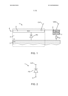
- A photodiode design that incorporates an insulation device in the semiconductor substrate to delimit the diffusion area, reducing the contribution of diffusion current and enhancing the drift current component, thereby increasing bandwidth and maintaining sensitivity constancy across wavelengths.
Photodiode and read-out circuit for a photodiode
PatentWO2020193553A1
Innovation
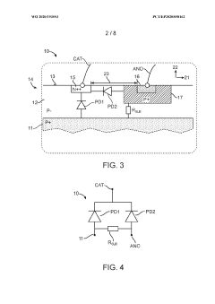
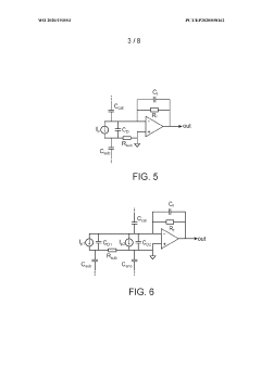
- A photodiode with a lateral structure featuring a semiconductor substrate and layer with laterally offset regions of opposite conductivity types, reducing capacitive couplings and noise amplification, and a readout circuit incorporating a transimpedance amplifier and high-pass filter to enhance signal-to-noise ratio and measurement accuracy.

Material Science Impacts on Photodiode Performance
Material science plays a crucial role in shaping the performance characteristics of photodiodes, directly impacting their data throughput capabilities. The choice of semiconductor materials and their properties significantly influence the device's responsivity, speed, and overall efficiency.
Silicon has long been the dominant material for photodiodes due to its abundance, low cost, and compatibility with existing semiconductor manufacturing processes. However, its inherent limitations in terms of bandgap and absorption coefficient have led researchers to explore alternative materials for enhanced performance.
Germanium, with its smaller bandgap, offers improved sensitivity in the near-infrared region, making it particularly suitable for telecommunications applications. Its higher carrier mobility also contributes to faster response times, potentially increasing data throughput in high-speed optical communication systems.
III-V compound semiconductors, such as gallium arsenide (GaAs) and indium gallium arsenide (InGaAs), have gained prominence in photodiode design. These materials exhibit superior electron mobility and can be engineered to have specific bandgaps, allowing for optimized performance across different wavelength ranges. InGaAs, in particular, has become the material of choice for long-wavelength applications due to its excellent responsivity in the 1.3-1.6 μm range.
Recent advancements in material science have led to the development of novel structures and compositions. Quantum dot photodetectors, utilizing nanoscale semiconductor particles, offer the potential for enhanced absorption and carrier multiplication, potentially leading to higher quantum efficiency and improved signal-to-noise ratios.
Two-dimensional materials, such as graphene and transition metal dichalcogenides (TMDs), have emerged as promising candidates for next-generation photodetectors. Their unique electronic properties, including high carrier mobility and tunable bandgaps, could enable ultrafast photoresponse and broadband detection capabilities.
The integration of plasmonic nanostructures with conventional semiconductor materials has shown promise in enhancing light absorption and carrier collection efficiency. By manipulating the interaction between light and metal nanoparticles, these hybrid materials can potentially overcome the trade-off between absorption efficiency and carrier transit time, leading to improved data throughput.
As material science continues to evolve, the development of new compounds, alloys, and nanostructured materials is expected to push the boundaries of photodiode performance. These advancements will likely lead to devices with higher sensitivity, faster response times, and broader spectral coverage, ultimately enabling higher data throughput in various applications ranging from optical communications to imaging systems.
Integration Challenges in High-Speed Systems
The integration of high-speed photodiodes into modern communication systems presents several significant challenges. One of the primary concerns is the management of parasitic capacitance and inductance, which can severely limit the bandwidth and response time of the photodiode. As data rates continue to increase, even small parasitic elements can cause signal distortion and limit the overall system performance.
Another critical challenge is the thermal management of high-speed photodiodes. The high current densities and power dissipation associated with these devices can lead to thermal runaway and reliability issues if not properly addressed. Designers must carefully consider heat dissipation mechanisms and implement effective cooling strategies to maintain stable operation and extend device lifetime.
Signal integrity is a paramount concern in high-speed systems. The integration of photodiodes with amplifiers and other circuit elements must be carefully optimized to minimize noise, crosstalk, and signal reflections. This often requires sophisticated packaging techniques and the use of impedance-matched transmission lines to preserve signal quality.
The choice of materials and fabrication processes also plays a crucial role in addressing integration challenges. Advanced semiconductor materials, such as III-V compounds, offer superior performance but can be difficult to integrate with silicon-based electronics. Hybrid integration approaches, such as flip-chip bonding or wafer-level packaging, are often employed to combine different material systems effectively.
Power consumption is another significant consideration in high-speed photodiode integration. As data rates increase, so does the power required to operate these devices. Balancing performance with power efficiency is essential, particularly in applications with strict power budgets or thermal constraints.
Scalability and cost-effectiveness present additional challenges in high-volume applications. Integrating high-performance photodiodes while maintaining manufacturability and yield requires careful consideration of design trade-offs and process compatibility. Techniques such as monolithic integration or silicon photonics are being explored to address these challenges and enable more cost-effective solutions.
Finally, the integration of high-speed photodiodes must also consider electromagnetic compatibility (EMC) and shielding requirements. The high-frequency signals generated by these devices can potentially interfere with other system components or be susceptible to external electromagnetic interference. Proper shielding, grounding, and layout techniques are essential to ensure robust operation in complex system environments.
Unlock deeper insights with PatSnap Eureka Quick Research — get a full tech report to explore trends and direct your research. Try now!
Generate Your Research Report Instantly with AI Agent
Supercharge your innovation with PatSnap Eureka AI Agent Platform!