Photodiode capability extension through hybrid electronics
AUG 21, 202510 MIN READ
Generate Your Research Report Instantly with AI Agent
Patsnap Eureka helps you evaluate technical feasibility & market potential.
Photodiode Evolution
Photodiodes have undergone significant evolution since their inception in the early 20th century. The journey began with the discovery of the photoelectric effect by Heinrich Hertz in 1887, which laid the foundation for photodiode technology. The first practical photodiodes were developed in the 1940s, utilizing selenium and silicon materials.
The 1950s marked a crucial turning point with the introduction of p-n junction photodiodes. These devices offered improved sensitivity and faster response times compared to their predecessors. The development of silicon-based photodiodes in the 1960s further revolutionized the field, providing enhanced performance and reliability.
The 1970s and 1980s saw rapid advancements in photodiode technology. PIN (Positive-Intrinsic-Negative) photodiodes emerged, offering lower capacitance and improved high-frequency response. Avalanche photodiodes (APDs) were also developed during this period, providing internal gain and higher sensitivity for low-light applications.
The 1990s brought about the integration of photodiodes with other electronic components, paving the way for more compact and efficient optoelectronic devices. This integration trend continued into the 2000s, with the development of advanced packaging techniques and the incorporation of photodiodes into complex integrated circuits.
In recent years, the focus has shifted towards enhancing the capabilities of photodiodes through hybrid electronics. This approach combines traditional photodiode technology with novel materials and fabrication techniques to overcome limitations in spectral response, speed, and sensitivity. Researchers are exploring the use of nanomaterials, such as quantum dots and graphene, to extend the spectral range and improve the overall performance of photodiodes.
The evolution of photodiodes has also been driven by the demands of emerging applications. In the field of telecommunications, high-speed photodiodes capable of operating at gigahertz frequencies have been developed to support fiber-optic networks. In medical imaging, specialized photodiodes with enhanced sensitivity in the near-infrared region have enabled advancements in non-invasive diagnostic techniques.
Looking ahead, the future of photodiode evolution lies in further integration with hybrid electronics. This includes the development of flexible and stretchable photodiodes for wearable technologies, as well as the incorporation of artificial intelligence and machine learning algorithms to enhance signal processing and detection capabilities. The ongoing research in materials science and nanotechnology is expected to yield new types of photodiodes with unprecedented performance characteristics, opening up possibilities for novel applications in fields such as quantum computing and advanced sensing systems.
Market Demand Analysis
The market demand for enhanced photodiode capabilities through hybrid electronics is experiencing significant growth, driven by the increasing need for high-performance sensing and detection systems across various industries. The integration of hybrid electronics with photodiodes offers substantial improvements in sensitivity, speed, and functionality, opening up new applications and market opportunities.
In the healthcare sector, there is a rising demand for advanced medical imaging and diagnostic tools. Hybrid photodiodes with extended capabilities are crucial for developing more accurate and efficient medical devices, such as PET scanners, endoscopes, and wearable health monitors. The global medical imaging market, which heavily relies on photodiode technology, is projected to expand rapidly in the coming years, creating a substantial demand for improved photodiode solutions.
The automotive industry is another key driver of market demand for enhanced photodiodes. With the growing adoption of advanced driver assistance systems (ADAS) and autonomous vehicles, there is an increasing need for high-performance light detection and ranging (LiDAR) systems. Hybrid photodiodes offer improved sensitivity and faster response times, which are essential for accurate object detection and distance measurement in automotive applications.
In the telecommunications sector, the ongoing rollout of 5G networks and the increasing demand for high-speed data transmission are fueling the need for advanced optical communication systems. Hybrid photodiodes with extended capabilities play a crucial role in improving the performance of optical receivers, enabling faster and more reliable data transmission over fiber optic networks.
The aerospace and defense industries also contribute significantly to the market demand for enhanced photodiodes. These sectors require highly sensitive and robust sensing solutions for applications such as target acquisition, missile guidance, and surveillance systems. Hybrid photodiodes offer improved performance in challenging environments, making them ideal for military and aerospace applications.
Furthermore, the growing adoption of Internet of Things (IoT) devices and smart home technologies is creating new opportunities for photodiode applications. Enhanced photodiodes are essential for developing more accurate and energy-efficient ambient light sensors, proximity sensors, and gesture recognition systems, which are increasingly integrated into consumer electronics and smart home devices.
The industrial automation sector is another area driving demand for advanced photodiode solutions. As manufacturing processes become more sophisticated and automated, there is a growing need for high-precision sensing and quality control systems. Hybrid photodiodes with extended capabilities enable the development of more accurate and reliable machine vision systems, optical inspection tools, and process control sensors.
Overall, the market demand for photodiode capability extension through hybrid electronics is expected to continue its upward trajectory, driven by technological advancements and the increasing need for high-performance sensing solutions across multiple industries. This trend presents significant opportunities for innovation and market growth in the coming years.
Current Limitations
Photodiodes have been widely used in various applications due to their ability to convert light into electrical signals. However, current photodiode technologies face several limitations that hinder their performance and broader adoption. These limitations primarily stem from the inherent properties of semiconductor materials and the traditional fabrication processes used in their production.
One of the most significant limitations is the restricted spectral response range of conventional photodiodes. Silicon-based photodiodes, which are the most common, typically operate effectively in the visible to near-infrared spectrum (400-1100 nm). This narrow range limits their applicability in fields requiring detection of ultraviolet or far-infrared radiation, such as astronomical observations or thermal imaging.
Another critical limitation is the trade-off between sensitivity and response speed. Increasing the thickness of the depletion region in a photodiode can improve its sensitivity, but this comes at the cost of reduced response speed due to increased carrier transit time. This trade-off poses challenges in applications requiring both high sensitivity and fast response times, such as high-speed optical communications.
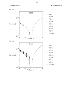
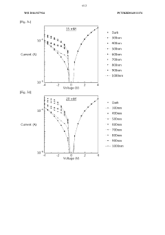
The dark current, which is the small electric current that flows through photosensitive devices even when no photons are entering the device, is another limiting factor. This unwanted current contributes to noise and reduces the signal-to-noise ratio, especially in low-light conditions. Minimizing dark current while maintaining other performance parameters remains a significant challenge in photodiode design.
Temperature sensitivity is also a considerable limitation for many photodiode applications. The performance of photodiodes can vary significantly with temperature changes, affecting their responsivity, dark current, and spectral response. This temperature dependence necessitates complex compensation mechanisms in many precision applications, increasing system complexity and cost.
Furthermore, the quantum efficiency of photodiodes, which represents the number of electron-hole pairs generated per incident photon, is not ideal across all wavelengths. This efficiency drop-off at certain wavelengths limits the overall sensitivity and effectiveness of photodiodes in specific applications.
The physical size of photodiodes also presents limitations, particularly in miniaturized or integrated systems. As devices become smaller, it becomes increasingly challenging to maintain high performance, especially in terms of sensitivity and noise characteristics. This size constraint impacts the integration of high-performance photodiodes in compact optoelectronic systems.
Lastly, the current manufacturing processes for high-performance photodiodes often involve complex and costly procedures, limiting their widespread adoption in cost-sensitive applications. The need for specialized materials and precise fabrication techniques contributes to higher production costs and potential scalability issues.
One of the most significant limitations is the restricted spectral response range of conventional photodiodes. Silicon-based photodiodes, which are the most common, typically operate effectively in the visible to near-infrared spectrum (400-1100 nm). This narrow range limits their applicability in fields requiring detection of ultraviolet or far-infrared radiation, such as astronomical observations or thermal imaging.
Another critical limitation is the trade-off between sensitivity and response speed. Increasing the thickness of the depletion region in a photodiode can improve its sensitivity, but this comes at the cost of reduced response speed due to increased carrier transit time. This trade-off poses challenges in applications requiring both high sensitivity and fast response times, such as high-speed optical communications.
The dark current, which is the small electric current that flows through photosensitive devices even when no photons are entering the device, is another limiting factor. This unwanted current contributes to noise and reduces the signal-to-noise ratio, especially in low-light conditions. Minimizing dark current while maintaining other performance parameters remains a significant challenge in photodiode design.
Temperature sensitivity is also a considerable limitation for many photodiode applications. The performance of photodiodes can vary significantly with temperature changes, affecting their responsivity, dark current, and spectral response. This temperature dependence necessitates complex compensation mechanisms in many precision applications, increasing system complexity and cost.
Furthermore, the quantum efficiency of photodiodes, which represents the number of electron-hole pairs generated per incident photon, is not ideal across all wavelengths. This efficiency drop-off at certain wavelengths limits the overall sensitivity and effectiveness of photodiodes in specific applications.
The physical size of photodiodes also presents limitations, particularly in miniaturized or integrated systems. As devices become smaller, it becomes increasingly challenging to maintain high performance, especially in terms of sensitivity and noise characteristics. This size constraint impacts the integration of high-performance photodiodes in compact optoelectronic systems.
Lastly, the current manufacturing processes for high-performance photodiodes often involve complex and costly procedures, limiting their widespread adoption in cost-sensitive applications. The need for specialized materials and precise fabrication techniques contributes to higher production costs and potential scalability issues.
Hybrid Electronics
01 Enhanced light sensitivity and detection
Photodiodes are designed with improved structures and materials to enhance their light sensitivity and detection capabilities. This includes optimizing the active area, reducing dark current, and implementing advanced semiconductor technologies to achieve higher quantum efficiency and responsivity across a wide spectral range.- Enhanced light sensitivity and detection: Photodiodes are designed with improved structures and materials to enhance their light sensitivity and detection capabilities. This includes optimizing the active area, reducing dark current, and implementing advanced semiconductor technologies to increase quantum efficiency and responsivity across a wide spectral range.
- Integration with readout circuits: Photodiodes are integrated with advanced readout circuits to improve signal processing and noise reduction. This integration enables features such as on-chip amplification, analog-to-digital conversion, and pixel-level processing, enhancing the overall performance and functionality of photodiode-based imaging systems.
- Specialized photodiode structures: Various specialized photodiode structures are developed to cater to specific applications. These include avalanche photodiodes for high-sensitivity detection, PIN photodiodes for improved response time, and heterojunction photodiodes for enhanced spectral selectivity. Such structures enable photodiodes to meet diverse requirements in different fields.
- Wavelength-specific photodiodes: Photodiodes are engineered to be sensitive to specific wavelengths or ranges of light. This is achieved through the use of specialized materials, optical filters, and innovative device structures. These wavelength-specific photodiodes find applications in areas such as spectroscopy, color sensing, and multi-spectral imaging.
- Miniaturization and array configuration: Advancements in photodiode technology focus on miniaturization and the ability to create dense arrays. This enables the development of high-resolution image sensors, compact spectrometers, and other applications requiring multiple photodiodes in a small form factor. Techniques such as 3D integration and advanced packaging are employed to achieve these goals.
02 Integration with readout circuits
Photodiodes are integrated with advanced readout circuits to improve signal processing and noise reduction. This integration enables features such as on-chip amplification, analog-to-digital conversion, and pixel-level processing, resulting in enhanced dynamic range and improved signal-to-noise ratio for various imaging and sensing applications.Expand Specific Solutions03 Specialized photodiode structures
Various specialized photodiode structures are developed to cater to specific applications. These include avalanche photodiodes for low-light detection, PIN photodiodes for high-speed applications, and heterojunction photodiodes for improved spectral response. Such structures enable photodiodes to meet diverse requirements in fields like telecommunications, spectroscopy, and scientific instrumentation.Expand Specific Solutions04 Multi-spectral and hyperspectral imaging
Photodiodes are designed to enable multi-spectral and hyperspectral imaging capabilities. This involves developing arrays of photodiodes with different spectral sensitivities or implementing tunable filters to capture light across multiple wavelength bands. These advancements allow for applications in remote sensing, medical imaging, and industrial inspection.Expand Specific Solutions05 High-speed operation and bandwidth
Photodiodes are optimized for high-speed operation and increased bandwidth. This involves reducing parasitic capacitances, implementing advanced materials, and optimizing device geometries. These improvements enable photodiodes to be used in high-speed optical communication systems, LiDAR applications, and time-of-flight sensors.Expand Specific Solutions
Key Industry Players
The research on photodiode capability extension through hybrid electronics is in a dynamic phase, with significant market potential and technological advancements. The industry is transitioning from early-stage development to more mature applications, driven by increasing demand for high-performance sensing and imaging solutions. The global market for advanced photodiodes is expanding rapidly, fueled by applications in telecommunications, healthcare, and consumer electronics. Technologically, companies like Hamamatsu Photonics, Sony Group, and Samsung SDI are leading the charge, leveraging their expertise in optoelectronics and semiconductor manufacturing to push the boundaries of photodiode capabilities. Emerging players such as Aeponyx and Nexeon are also contributing innovative approaches, particularly in integrating MEMS and silicon photonics technologies with traditional photodiode designs.
Hamamatsu Photonics KK
Technical Solution: Hamamatsu Photonics has developed a hybrid photodiode technology that combines traditional silicon photodiodes with novel materials to extend their capabilities. Their approach utilizes a thin film of organic semiconductors deposited on top of silicon photodiodes, creating a hybrid structure that enhances sensitivity and expands the detectable wavelength range[1]. This technology allows for improved near-infrared detection, crucial for applications in spectroscopy and medical imaging. The company has also integrated on-chip circuitry with their hybrid photodiodes, enabling advanced functionalities such as time-gated detection and improved signal processing[2]. Hamamatsu's hybrid photodiodes demonstrate enhanced quantum efficiency across a broader spectrum, with reported improvements of up to 40% in the near-infrared region compared to conventional silicon photodiodes[3].
Strengths: Expanded wavelength sensitivity, improved quantum efficiency, and integrated advanced functionalities. Weaknesses: Potentially higher production costs and complexity in manufacturing processes compared to traditional photodiodes.
ams-Osram International GmbH
Technical Solution: ams-Osram has pioneered a hybrid photodiode technology that integrates multiple sensing capabilities into a single chip. Their approach combines traditional photodiode structures with specialized materials and micro-optics to create multi-functional sensors. The company has developed a hybrid sensor that incorporates both visible light sensing and proximity detection, utilizing a unique stack of materials that includes silicon and III-V compound semiconductors[4]. This hybrid design allows for simultaneous ambient light and proximity sensing, reducing component count and power consumption in mobile devices. ams-Osram has also introduced hybrid photodiodes with integrated filters and lenses, enabling spectral selectivity and improved light collection efficiency[5]. Their technology demonstrates a 30% reduction in package size compared to discrete solutions while maintaining high performance[6].
Strengths: Multi-functional sensing capabilities, reduced component count, and improved integration for mobile devices. Weaknesses: Potential challenges in balancing performance across different sensing modalities and higher initial development costs.
Core Innovations
Photodiode using graphene-silicon quantum dot hybrid structure and method of manufacturing the same
PatentActiveUS10056520B2
Innovation
- A graphene-silicon quantum dot hybrid structure is developed, where silicon quantum dots are formed in a silicon oxide thin film and doped graphene is applied on top, allowing for control of energy bandgap and Fermi level, enabling wide photodetection from ultraviolet to near-infrared regions with reduced operating voltage.
Photodiode using graphene-silicon quantum dot hybrid structure and method for preparing same
PatentWO2016027934A1
Innovation
- A graphene-silicon quantum dot hybrid structure is developed, where silicon quantum dots are formed in a silicon oxide thin film and doped graphene is applied, allowing for control of energy band gap and Fermi level, enabling wide photodetection from ultraviolet to near-infrared and optimizing performance through size control of quantum dots and doping concentration.
Manufacturing Challenges
The manufacturing challenges associated with extending photodiode capabilities through hybrid electronics are multifaceted and require innovative solutions. One of the primary obstacles is the integration of disparate materials and components, each with unique processing requirements. The fabrication of hybrid photodiodes often involves combining traditional semiconductor materials with novel organic or inorganic compounds, which can lead to compatibility issues during manufacturing.
Temperature sensitivity presents another significant challenge. Many of the materials used in hybrid photodiodes have different thermal expansion coefficients, potentially causing stress and delamination during high-temperature processing steps. This necessitates the development of low-temperature fabrication techniques or advanced thermal management strategies to maintain the integrity of the device structure.
Precision alignment and bonding of different layers and components are critical for optimal device performance. Achieving consistent and accurate alignment at the micro or nanoscale across large production volumes remains a formidable task. Advanced lithography and pick-and-place technologies are being explored to address this issue, but further refinement is needed to meet the demanding requirements of hybrid photodiode manufacturing.
Contamination control is paramount in the production of high-performance photodiodes. The introduction of new materials and processes in hybrid designs increases the risk of contamination, potentially compromising device sensitivity and reliability. Stringent cleanroom protocols and specialized handling equipment are essential to mitigate these risks, adding complexity and cost to the manufacturing process.
Scalability poses a significant challenge in transitioning from laboratory prototypes to mass production. Many of the techniques used to create high-performance hybrid photodiodes in research settings are not readily adaptable to high-volume manufacturing environments. Developing scalable processes that maintain device quality and consistency across large production runs is a key focus area for industry researchers and engineers.
Quality control and testing procedures must be adapted to accommodate the unique characteristics of hybrid photodiodes. Traditional testing methods may not adequately capture the performance metrics of these advanced devices, necessitating the development of new inspection and characterization techniques. This includes non-destructive testing methods capable of evaluating the complex internal structures of hybrid photodiodes without compromising their integrity.
Lastly, the cost-effectiveness of manufacturing processes remains a critical consideration. While hybrid photodiodes offer enhanced capabilities, their production often involves more complex and expensive manufacturing steps compared to conventional photodiodes. Balancing performance improvements against manufacturing costs is essential for commercial viability, driving ongoing efforts to optimize production techniques and explore alternative materials and designs that can deliver similar performance enhancements with reduced manufacturing complexity.
Sustainability Impact
The integration of photodiodes with hybrid electronics presents significant opportunities for enhancing sustainability across various sectors. By extending the capabilities of photodiodes through hybrid electronics, we can achieve more efficient energy harvesting, improved sensor performance, and reduced material consumption, all of which contribute to a more sustainable future.
In the realm of energy harvesting, hybrid photodiode systems can significantly increase the efficiency of solar cells. By combining traditional silicon-based photodiodes with emerging organic or perovskite materials, we can create multi-junction solar cells that capture a broader spectrum of light. This results in higher conversion efficiencies and reduced reliance on non-renewable energy sources. Additionally, the use of flexible hybrid electronics allows for the development of lightweight, portable solar panels that can be integrated into a wide range of products, from wearable devices to building materials.
The enhanced sensitivity and spectral range of hybrid photodiodes also have implications for environmental monitoring and conservation efforts. These advanced sensors can detect minute changes in light intensity and wavelength, enabling more accurate measurements of air and water quality, as well as early detection of pollutants. This improved monitoring capability can lead to more timely and effective environmental interventions, helping to preserve ecosystems and biodiversity.
In the agricultural sector, hybrid photodiode technology can contribute to sustainable farming practices. By developing highly sensitive light sensors, farmers can optimize crop growth conditions, reducing the need for water, fertilizers, and pesticides. These sensors can be integrated into smart irrigation systems and automated greenhouses, maximizing resource efficiency and minimizing environmental impact.
The miniaturization and increased functionality of hybrid photodiodes also support the development of more sustainable consumer electronics. By incorporating these advanced sensors into smartphones, tablets, and other devices, manufacturers can create products with longer lifespans and reduced energy consumption. Features such as adaptive display brightness and improved camera performance not only enhance user experience but also contribute to energy conservation.
Furthermore, the use of hybrid electronics in photodiode production can lead to more sustainable manufacturing processes. The combination of traditional silicon-based fabrication with additive manufacturing techniques for organic components can reduce material waste and energy consumption during production. This approach also opens up possibilities for easier recycling and recovery of valuable materials at the end of a product's life cycle.
In conclusion, the extension of photodiode capabilities through hybrid electronics has the potential to drive significant advancements in sustainability across multiple industries. From renewable energy and environmental monitoring to sustainable agriculture and eco-friendly consumer electronics, this technology promises to play a crucial role in building a more sustainable future.
Unlock deeper insights with Patsnap Eureka Quick Research — get a full tech report to explore trends and direct your research. Try now!
Generate Your Research Report Instantly with AI Agent
Supercharge your innovation with Patsnap Eureka AI Agent Platform!