High-resolution imaging capabilities with advanced photodiodes
AUG 21, 20259 MIN READ
Generate Your Research Report Instantly with AI Agent
Patsnap Eureka helps you evaluate technical feasibility & market potential.
Photodiode Imaging Evolution
The evolution of photodiode imaging technology has been marked by significant advancements in resolution, sensitivity, and integration capabilities. Initially developed in the mid-20th century, photodiodes have undergone a remarkable transformation, transitioning from simple light-sensing components to sophisticated imaging devices capable of high-resolution image capture.
In the early stages, photodiodes were primarily used for basic light detection and measurement applications. The 1960s and 1970s saw the emergence of silicon-based photodiodes, which offered improved sensitivity and reliability compared to their predecessors. This period laid the foundation for the development of more advanced imaging applications.
The 1980s and 1990s witnessed a surge in research and development efforts focused on enhancing the performance of photodiodes for imaging purposes. During this time, significant progress was made in reducing noise levels, increasing quantum efficiency, and improving the overall signal-to-noise ratio of photodiode-based imaging systems.
The turn of the millennium marked a pivotal point in photodiode imaging evolution. The introduction of CMOS (Complementary Metal-Oxide-Semiconductor) image sensors revolutionized the field, enabling the integration of photodiodes with on-chip readout circuitry. This integration led to substantial improvements in image quality, power efficiency, and manufacturing costs.
In recent years, the focus has shifted towards developing advanced photodiode structures and materials to push the boundaries of imaging capabilities. Novel designs such as back-illuminated sensors, stacked sensor architectures, and the use of alternative semiconductor materials have contributed to significant enhancements in resolution, dynamic range, and low-light performance.
The advent of machine learning and artificial intelligence has further accelerated the evolution of photodiode imaging. These technologies have enabled sophisticated image processing algorithms that can extract more information from raw sensor data, leading to improvements in image quality, color accuracy, and noise reduction.
Looking ahead, the future of photodiode imaging is poised for continued innovation. Emerging technologies such as quantum dot photodiodes, organic photodiodes, and hybrid organic-inorganic structures hold promise for achieving even higher resolutions and sensitivities. Additionally, the integration of photodiodes with other sensing modalities, such as spectral imaging and 3D sensing, is expected to open up new possibilities for advanced imaging applications across various industries.
High-Res Imaging Market Demand
The market demand for high-resolution imaging capabilities with advanced photodiodes has been experiencing significant growth across various industries. This surge is primarily driven by the increasing need for superior image quality in applications ranging from consumer electronics to industrial and medical imaging.
In the consumer electronics sector, smartphone manufacturers are constantly pushing the boundaries of camera technology to meet the growing expectations of users for high-quality photos and videos. Advanced photodiodes play a crucial role in enhancing low-light performance, dynamic range, and overall image fidelity. The demand for better selfie cameras and multi-camera setups has further fueled the need for high-resolution imaging solutions.
The automotive industry represents another major market for high-resolution imaging technologies. With the advent of advanced driver assistance systems (ADAS) and autonomous vehicles, there is a growing requirement for high-performance image sensors capable of capturing detailed environmental data in various lighting conditions. These sensors, equipped with advanced photodiodes, are essential for features such as lane departure warnings, pedestrian detection, and adaptive cruise control.
In the healthcare sector, medical imaging devices such as endoscopes, surgical microscopes, and diagnostic equipment benefit greatly from high-resolution imaging capabilities. The demand for minimally invasive procedures and accurate diagnostic tools has led to increased adoption of advanced imaging technologies. Improved photodiodes enable better visualization of fine details, enhancing the precision of medical procedures and diagnoses.
The security and surveillance market also contributes significantly to the demand for high-resolution imaging. As public safety concerns grow, there is an increasing need for high-quality video surveillance systems capable of capturing clear images in challenging lighting conditions. Advanced photodiodes enable better low-light performance and wider dynamic range, crucial for effective monitoring in various environments.
Industrial inspection and quality control processes have embraced high-resolution imaging to improve efficiency and accuracy. In manufacturing, advanced photodiodes enable the detection of minute defects and ensure precise measurements. The food and pharmaceutical industries rely on high-resolution imaging for product inspection and contamination detection.
The scientific research community represents another significant market segment. Fields such as astronomy, microscopy, and spectroscopy require cutting-edge imaging capabilities to push the boundaries of scientific discovery. Advanced photodiodes contribute to improved sensitivity and resolution in these applications, enabling researchers to observe phenomena at unprecedented levels of detail.
As the Internet of Things (IoT) continues to expand, the demand for high-resolution imaging in smart devices and sensors is expected to grow. From smart home security cameras to agricultural monitoring systems, the need for reliable and high-quality imaging solutions is increasing across various IoT applications.
Photodiode Tech Challenges
The development of high-resolution imaging capabilities with advanced photodiodes faces several significant technical challenges. One of the primary obstacles is the trade-off between sensitivity and speed. As pixel sizes decrease to achieve higher resolution, the amount of light captured by each pixel reduces, leading to lower sensitivity. This necessitates longer exposure times, which can result in motion blur and reduced frame rates.
Another challenge lies in the management of noise, particularly in low-light conditions. As photodiodes become more sensitive to capture finer details, they also become more susceptible to various types of noise, including shot noise, dark current noise, and read noise. Mitigating these noise sources without compromising image quality or speed remains a complex engineering problem.
The fabrication of advanced photodiodes with consistent performance across large arrays presents manufacturing difficulties. Achieving uniformity in terms of quantum efficiency, dark current, and spectral response across millions of pixels is crucial for high-quality imaging but becomes increasingly challenging as pixel sizes shrink and array sizes grow.
Power consumption is another significant concern, especially for portable devices and high-speed imaging applications. The need for on-chip processing to handle the increased data throughput from high-resolution sensors can lead to substantial power requirements, which must be balanced against battery life and heat dissipation constraints.
Addressing color accuracy and dynamic range limitations also poses challenges. Traditional Bayer filter arrays used for color imaging can reduce overall sensitivity and introduce color artifacts. Developing alternative color sensing technologies or improving color reconstruction algorithms is necessary to enhance color fidelity in high-resolution imaging.
The integration of advanced photodiodes with readout circuitry presents additional complexities. As pixel densities increase, the design of efficient charge transfer mechanisms and analog-to-digital converters becomes more critical to maintain high frame rates and low noise levels.
Lastly, the development of suitable optics to match the resolution capabilities of advanced photodiodes is a significant challenge. Lens designs must evolve to provide sufficient resolving power and minimal aberrations across the entire image sensor, which becomes increasingly difficult as sensor resolutions push beyond the diffraction limit of conventional optics.
Overcoming these technical challenges requires interdisciplinary approaches, combining advancements in semiconductor physics, materials science, signal processing, and optical engineering. The successful resolution of these issues will pave the way for next-generation imaging systems with unprecedented resolution and performance.
Current High-Res Solutions
01 Advanced photodiode structures for improved imaging resolution
Novel photodiode designs and structures are developed to enhance imaging resolution. These include optimized doping profiles, reduced pixel sizes, and innovative junction configurations that minimize crosstalk and improve light sensitivity. Such advancements allow for higher pixel densities and sharper image quality in various imaging applications.- Advanced photodiode structures for improved imaging resolution: Novel photodiode designs and structures are developed to enhance imaging resolution. These include optimized pixel architectures, back-illuminated sensors, and stacked photodiode layers. Such advancements allow for increased light sensitivity, reduced noise, and improved spatial resolution in imaging devices.
- Image processing techniques for resolution enhancement: Various image processing algorithms and techniques are employed to improve the effective resolution of photodiode-based imaging systems. These may include super-resolution algorithms, image reconstruction methods, and advanced signal processing techniques to extract more detail from raw sensor data.
- High-speed readout and data processing for improved resolution: Advanced readout circuits and high-speed data processing techniques are implemented to increase the frame rate and reduce motion blur in photodiode imaging systems. This allows for capturing more frames and combining them to enhance overall image resolution and quality.
- Pixel-level innovations for resolution enhancement: Innovations at the pixel level, such as sub-pixel arrangements, micro-lenses, and color filter arrays, are developed to improve the effective resolution of photodiode-based image sensors. These techniques allow for capturing more spatial information within the same sensor area.
- Integration of advanced materials and fabrication techniques: Novel materials and fabrication techniques are employed in photodiode manufacturing to enhance their performance and resolution capabilities. This includes the use of advanced semiconductor materials, nanomaterials, and precision fabrication processes to create more efficient and sensitive photodiodes.
02 Image processing techniques for resolution enhancement
Sophisticated image processing algorithms are employed to improve the effective resolution of photodiode-based imaging systems. These techniques include super-resolution methods, noise reduction, and advanced interpolation algorithms that can extract more detail from raw sensor data, resulting in sharper and more detailed images.Expand Specific Solutions03 Multi-layer and 3D photodiode architectures
Innovative multi-layer and three-dimensional photodiode architectures are developed to increase light absorption efficiency and improve spatial resolution. These designs allow for better light management, reduced pixel crosstalk, and increased quantum efficiency, leading to enhanced imaging performance in compact form factors.Expand Specific Solutions04 Integration of micro-lenses and light guides
Micro-lenses and light guides are integrated with photodiode arrays to improve light collection efficiency and reduce pixel crosstalk. These optical elements help focus incident light onto the active areas of photodiodes, increasing sensitivity and enabling higher resolution imaging, particularly in low-light conditions.Expand Specific Solutions05 Advanced readout circuits and signal processing
Sophisticated readout circuits and signal processing techniques are developed to maximize the performance of high-resolution photodiode arrays. These include low-noise amplifiers, high-speed analog-to-digital converters, and on-chip signal processing capabilities that enable faster readout speeds, improved dynamic range, and enhanced overall image quality.Expand Specific Solutions
Key Photodiode Manufacturers
The research on high-resolution imaging capabilities with advanced photodiodes is in a mature stage, with significant market growth potential. The global market for advanced photodiodes is expanding rapidly, driven by increasing demand in various sectors such as automotive, healthcare, and consumer electronics. Key players like OmniVision Technologies, Samsung Electronics, and Sony Semiconductor Solutions are leading the field with innovative technologies. Companies such as OSRAM Opto Semiconductors and Hamamatsu Photonics are also making substantial contributions. The competitive landscape is characterized by intense R&D efforts, with academic institutions like MIT and Tohoku University collaborating with industry leaders to push the boundaries of photodiode technology. This synergy between academia and industry is accelerating the development of next-generation imaging solutions, promising further advancements in resolution, sensitivity, and application versatility.
OmniVision Technologies, Inc.
Technical Solution: OmniVision has developed advanced CMOS image sensors with high-resolution capabilities. Their latest sensors feature a stacked die architecture, incorporating backside-illuminated (BSI) pixel arrays with sizes down to 0.56 μm[1]. This technology allows for higher pixel density and improved light sensitivity. OmniVision's photodiodes utilize deep trench isolation (DTI) to minimize crosstalk between adjacent pixels, resulting in enhanced image quality and color fidelity[2]. The company has also implemented on-chip HDR processing, enabling sensors to capture high dynamic range scenes with up to 140dB dynamic range[3].
Strengths: Industry-leading pixel size reduction, excellent low-light performance, and wide dynamic range. Weaknesses: Potential heat generation in high-density arrays, and higher production costs compared to traditional CMOS sensors.
Samsung Electronics Co., Ltd.
Technical Solution: Samsung has made significant strides in high-resolution imaging with their ISOCELL technology. Their latest sensors feature pixel sizes as small as 0.64μm, allowing for higher resolution in compact form factors[4]. The ISOCELL Plus technology uses a novel material to replace the metal grid between color filters, reducing light reflection and crosstalk[5]. Samsung has also developed Tetracell technology, which combines four pixels into one larger pixel for improved low-light performance while maintaining high resolution in bright conditions[6]. Additionally, their Dual Pixel Pro autofocus technology utilizes 100% of the sensor's pixels for faster and more accurate focusing[7].
Strengths: High pixel density, versatile performance across lighting conditions, and advanced autofocus capabilities. Weaknesses: Potential challenges in managing heat dissipation and power consumption in high-resolution sensors.
Photodiode Design Innovations
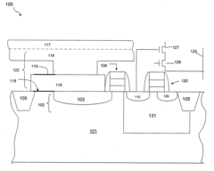
Four shared pixel with phase detection and horizontal and vertical binning readout modes
PatentActiveUS20230283918A1
Innovation
- The implementation of an imaging system with four photodiodes sharing a common readout amplifier, row select transistor, microlens, and color filter, allowing for horizontal or vertical binning, or both, to enhance autofocus functionality and improve frame rate and slow-motion imaging capabilities.
Raised photodiode sensor to increase fill factor and quantum efficiency in scaled pixels
PatentActiveUS20060175641A1
Innovation
- The use of a doped, hydrogenated amorphous silicon photosensor raised above the substrate surface, combined with inert implants like fluorine or deuterium, increases the fill factor and quantum efficiency by reducing leakage and barrier issues, and mitigates hysteresis effects.
Imaging Sensor Applications
Advanced photodiodes have revolutionized the field of imaging sensors, enabling a wide range of applications across various industries. These high-performance devices have significantly enhanced the capabilities of imaging systems, allowing for improved resolution, sensitivity, and speed in image capture.
In the medical field, advanced photodiodes have found extensive use in diagnostic imaging equipment. X-ray detectors utilizing these sensors provide higher-quality images with reduced radiation exposure for patients. Additionally, endoscopic cameras equipped with advanced photodiodes offer superior visualization during minimally invasive procedures, enhancing surgical precision and patient outcomes.
The automotive industry has also benefited greatly from the integration of advanced photodiodes in imaging sensors. Advanced driver assistance systems (ADAS) rely on these sensors for functions such as lane departure warnings, adaptive cruise control, and collision avoidance. The high-resolution imaging capabilities of advanced photodiodes enable more accurate object detection and tracking, contributing to improved vehicle safety and paving the way for autonomous driving technologies.
In the realm of scientific research, advanced photodiodes have enabled breakthroughs in fields such as astronomy and particle physics. Telescopes equipped with these sensors can capture images of distant celestial objects with unprecedented clarity and detail. Similarly, particle detectors in high-energy physics experiments utilize advanced photodiodes to track and analyze subatomic particles with exceptional precision.
The consumer electronics market has seen a surge in the adoption of advanced photodiodes in smartphone cameras. These sensors have dramatically improved low-light performance, enabling users to capture high-quality images in challenging lighting conditions. The enhanced resolution and dynamic range provided by advanced photodiodes have also contributed to the development of computational photography techniques, further pushing the boundaries of mobile imaging capabilities.
Industrial applications of advanced photodiodes include machine vision systems for quality control and inspection processes. The high-resolution imaging capabilities of these sensors allow for the detection of minute defects and anomalies in manufacturing processes, improving product quality and reducing waste. Additionally, advanced photodiodes have found applications in spectroscopy and colorimetry, enabling precise color measurement and analysis in industries such as printing, textiles, and food production.
In the field of security and surveillance, advanced photodiodes have significantly enhanced the capabilities of imaging systems. High-resolution cameras equipped with these sensors provide clearer images and improved facial recognition capabilities, contributing to more effective security measures in public spaces and critical infrastructure.
Quantum Efficiency Advances
Quantum efficiency (QE) has become a critical parameter in advancing high-resolution imaging capabilities with photodiodes. Recent developments in this field have led to significant improvements in the ability of photodiodes to convert incident photons into electrical signals, thereby enhancing overall image quality and sensitivity.
One of the key advancements in quantum efficiency has been the implementation of back-illuminated sensor designs. This approach allows incoming light to reach the photodiode's active region without being obstructed by metal interconnects or other structures typically present on the front side of the sensor. By eliminating these obstacles, back-illuminated sensors can achieve quantum efficiencies of up to 95% across a wide range of wavelengths, representing a substantial improvement over traditional front-illuminated designs.
Another area of progress has been the development of multi-layer photodiodes. These structures utilize different semiconductor materials stacked in layers, each optimized for specific wavelength ranges. This design enables the capture of a broader spectrum of light, resulting in improved quantum efficiency across the entire visible and near-infrared spectrum. Some advanced multi-layer photodiodes have demonstrated quantum efficiencies exceeding 80% from 400nm to 1000nm wavelengths.
Surface passivation techniques have also contributed significantly to quantum efficiency advancements. By reducing surface recombination of charge carriers, these methods minimize losses and increase the overall quantum efficiency of the photodiode. Advanced passivation techniques, such as atomic layer deposition of high-k dielectrics, have shown promise in achieving quantum efficiencies above 90% in the visible spectrum.
The integration of nanostructures, such as quantum dots and nanowires, into photodiode designs has opened up new possibilities for enhancing quantum efficiency. These nanostructures can be tailored to absorb light more effectively at specific wavelengths, potentially leading to quantum efficiencies approaching 100% for targeted spectral ranges. This technology is particularly promising for applications requiring high sensitivity in specific parts of the spectrum, such as low-light imaging or multispectral sensing.
Recent research has also focused on the development of organic and perovskite-based photodiodes, which offer the potential for high quantum efficiencies in flexible and large-area imaging applications. These materials have demonstrated quantum efficiencies exceeding 70% across the visible spectrum, with some narrow-band organic photodiodes achieving peak efficiencies of over 90%.
As quantum efficiency continues to improve, the challenge now lies in maintaining these high levels of performance while addressing other critical parameters such as dark current, response time, and pixel size. The ongoing research in this field promises to push the boundaries of high-resolution imaging capabilities, enabling new applications in fields ranging from scientific instrumentation to consumer electronics.
Unlock deeper insights with Patsnap Eureka Quick Research — get a full tech report to explore trends and direct your research. Try now!
Generate Your Research Report Instantly with AI Agent
Supercharge your innovation with Patsnap Eureka AI Agent Platform!