Quantum Tunneling Effects on Quasi-Static Device Operations
SEP 4, 20259 MIN READ
Generate Your Research Report Instantly with AI Agent
PatSnap Eureka helps you evaluate technical feasibility & market potential.
Quantum Tunneling Background and Objectives
Quantum tunneling represents one of the most fascinating phenomena in quantum mechanics, where particles penetrate energy barriers that would be insurmountable according to classical physics. This effect, first theorized in the early 20th century, has evolved from a theoretical curiosity to a critical consideration in modern electronic device design. The historical progression of quantum tunneling research began with wave mechanics formulations by Schrödinger and applications to nuclear physics by Gamow, eventually extending to solid-state physics and semiconductor behavior.
In contemporary electronic devices, particularly as dimensions shrink below 10nm, quantum tunneling transitions from a peripheral concern to a dominant factor affecting device performance. The exponential relationship between tunneling probability and barrier width means that even minor dimensional reductions can dramatically increase tunneling currents, fundamentally altering device characteristics that were previously governed by classical physics principles.
The technological landscape has been significantly impacted by quantum tunneling effects, both as limitations and opportunities. While tunneling-induced leakage currents present challenges for conventional CMOS technology scaling, they have also enabled innovative devices like tunnel field-effect transistors (TFETs) and resonant tunneling diodes (RTDs). These devices explicitly harness quantum tunneling for their operation, representing a paradigm shift from fighting quantum effects to exploiting them.
Current research trajectories focus on comprehensive modeling approaches that accurately capture tunneling phenomena across diverse material systems and device architectures. This includes developing multi-scale simulation frameworks that bridge quantum mechanical calculations with device-level performance metrics, enabling more accurate predictions of quasi-static operation parameters.
The primary objectives of investigating quantum tunneling effects on quasi-static device operations include: establishing quantitative relationships between device geometries and tunneling-induced behaviors; developing predictive models that can guide device optimization; identifying novel materials and structures that can either mitigate unwanted tunneling or enhance beneficial tunneling processes; and formulating design guidelines that account for quantum effects in next-generation electronic devices.
Additionally, research aims to explore the fundamental limits of deterministic device operation in the presence of quantum tunneling, particularly as dimensions approach atomic scales where quantum effects become increasingly probabilistic rather than deterministic. This understanding is crucial for establishing realistic expectations for future technology nodes and potentially discovering new operational paradigms that embrace quantum behavior rather than treating it as a limitation.
Market Applications for Quantum Tunneling Technologies
Quantum tunneling technologies are rapidly transitioning from theoretical physics concepts to practical market applications across multiple industries. The semiconductor industry represents the most mature market for quantum tunneling applications, with tunnel field-effect transistors (TFETs) emerging as promising alternatives to conventional MOSFETs. These devices leverage band-to-band tunneling to achieve subthreshold swing below the thermal limit of 60mV/decade, enabling ultra-low power consumption in integrated circuits. Market projections indicate that TFETs could capture up to 15% of the advanced logic market by 2030, particularly in IoT and edge computing applications where power efficiency is paramount.
In the emerging quantum computing sector, quantum tunneling serves as a fundamental mechanism for quantum bits (qubits) in superconducting quantum computers. Companies like IBM, Google, and Rigetti are commercializing systems that utilize Josephson junctions—where quantum tunneling occurs between superconductors separated by thin insulating barriers. This market segment is experiencing exponential growth, with annual investments exceeding $1 billion globally and projected compound annual growth rates above 30% through 2028.
Scanning tunneling microscopy (STM) represents another established commercial application, with a global market valued at approximately $570 million. Beyond traditional research applications, STM technologies are finding new commercial uses in semiconductor manufacturing quality control, materials science, and nanotechnology development. The ability to manipulate individual atoms through quantum tunneling is creating new possibilities for atomic-scale manufacturing processes.
Energy harvesting applications are gaining significant traction, particularly in resonant tunneling diodes for thermal energy conversion and quantum tunneling composite materials that change electrical resistance under mechanical pressure. These materials are finding applications in pressure sensors, touchscreens, and flexible electronics, with market growth rates exceeding 25% annually in specialized sensing applications.
Medical diagnostics represents an emerging application area where quantum tunneling biosensors offer unprecedented sensitivity for detecting biomarkers at molecular levels. These sensors can detect specific proteins, DNA sequences, or viral particles at concentrations orders of magnitude lower than conventional methods. Early commercial applications are appearing in rapid diagnostic testing, with several startups securing significant venture funding for commercialization efforts.
Quantum tunneling is also enabling advances in secure communications through quantum key distribution systems that leverage fundamental quantum properties for theoretically unbreakable encryption. This market segment is growing rapidly at over 20% annually, driven by increasing cybersecurity concerns across government, financial, and defense sectors requiring ultra-secure communication channels.
Current Challenges in Quasi-Static Device Operations
Quasi-static device operations face significant challenges due to the increasing influence of quantum tunneling effects as device dimensions continue to shrink. Traditional semiconductor devices operating in quasi-static regimes have historically relied on classical physics principles, but at sub-10nm scales, quantum mechanical phenomena become dominant, disrupting conventional operational models.
The most pressing challenge is the exponential increase in leakage current caused by quantum tunneling through potential barriers that were previously considered impenetrable in classical device physics. This phenomenon creates a fundamental limit to the scaling of conventional CMOS technology, as the off-state current becomes unacceptably high, leading to excessive power consumption even when devices are nominally switched off.
Gate oxide tunneling presents another critical issue, where electrons tunnel directly through the thin insulating layer between the gate and the channel. As gate oxides have been reduced to just a few atomic layers thick to maintain electrostatic control, the probability of tunneling increases dramatically, compromising the integrity of the gate control mechanism and introducing variability in device performance.
Band-to-band tunneling (BTBT) emerges as devices operate at lower voltages with steeper band bending. This creates additional leakage paths that are particularly problematic in highly-doped regions and at junction interfaces. The resulting parasitic currents significantly impact the reliability of quasi-static operational models and create discrepancies between theoretical predictions and actual device behavior.
Temperature dependence of tunneling effects introduces further complexity, as quantum tunneling exhibits different temperature sensitivities compared to classical thermal processes. This creates non-linear responses in device characteristics across operating temperature ranges, making it difficult to maintain consistent performance in varying environmental conditions.
Modeling challenges have become increasingly severe, as traditional compact models fail to accurately capture quantum effects in quasi-static operations. The industry lacks standardized approaches to incorporate quantum tunneling into device simulation frameworks, creating inconsistencies in design methodologies and performance predictions across different platforms.
Material interface effects compound these challenges, as atomic-level imperfections at boundaries between different materials create localized states that can enhance tunneling probabilities. These effects are stochastic in nature and difficult to control in manufacturing processes, leading to device-to-device variability that undermines the reliability of large-scale integrated circuits.
The time-dependent nature of tunneling phenomena also challenges the fundamental assumptions of quasi-static operation, introducing dynamic effects that occur at timescales relevant to circuit operation but are not captured by conventional quasi-static approximations.
Existing Solutions for Tunneling Effect Management
01 Quantum tunneling transistor design and operation
Quantum tunneling transistors utilize the quantum mechanical phenomenon where electrons tunnel through energy barriers that would be insurmountable in classical physics. These devices operate by controlling the tunneling probability through manipulation of barrier width, height, or applied voltage. The design typically includes source, drain, and gate regions with precisely engineered quantum barriers that allow for high-speed switching operations with reduced power consumption compared to conventional transistors.- Quantum tunneling transistor design and operation: Quantum tunneling transistors utilize the quantum mechanical phenomenon where electrons tunnel through energy barriers they classically couldn't overcome. These devices feature specialized gate structures that control the tunneling probability, allowing for switching operations at lower voltages than conventional transistors. The design typically includes thin barrier regions between source and drain, with precise material interfaces to facilitate controlled electron tunneling, resulting in improved energy efficiency and potentially faster switching speeds.
- Resonant tunneling diode implementations: Resonant tunneling diodes (RTDs) operate based on quantum tunneling through double or multiple barrier structures, creating negative differential resistance regions in their I-V characteristics. These devices contain quantum wells between barriers where electron energy levels become quantized, allowing resonant tunneling when the applied voltage aligns these energy levels with the electron energy in the emitter region. RTDs are implemented in high-frequency oscillators, logic circuits, and memory devices, offering advantages in speed and reduced power consumption compared to conventional semiconductor devices.
- Quantum tunneling in memory and computing applications: Quantum tunneling mechanisms are leveraged in advanced memory and computing architectures to achieve higher performance and novel functionalities. These applications include tunnel junction-based memory cells where data is stored based on the tunneling resistance state, quantum dot cellular automata that use electron tunneling for computation without current flow, and tunneling-based logic gates that can perform operations with reduced power consumption. The controlled tunneling of electrons enables non-volatile storage and processing capabilities that overcome limitations of conventional charge-based technologies.
- Quantum tunneling sensing and detection systems: Sensing and detection systems exploit quantum tunneling effects to achieve high sensitivity measurements. These devices typically use tunnel junctions whose electrical characteristics change in response to external stimuli such as electromagnetic fields, temperature variations, or molecular interactions. The exponential dependence of tunneling current on barrier width makes these sensors extremely sensitive to small physical changes. Applications include scanning tunneling microscopy, quantum-enhanced photodetectors, and specialized sensors for detecting specific molecules or radiation with precision beyond classical limits.
- Fabrication techniques for quantum tunneling devices: Advanced fabrication methods are essential for creating reliable quantum tunneling devices with precisely controlled barrier dimensions and material properties. These techniques include atomic layer deposition for creating ultra-thin barrier layers, molecular beam epitaxy for growing high-quality heterostructures with atomically sharp interfaces, and advanced lithography processes to define nanoscale features. Post-fabrication treatments are often employed to optimize tunneling characteristics by modifying interface states and reducing defects that could interfere with the quantum tunneling process.
02 Resonant tunneling diodes and oscillators
Resonant tunneling diodes (RTDs) operate based on quantum tunneling through double or multiple barrier structures. These devices exhibit negative differential resistance characteristics, making them suitable for high-frequency oscillator applications. The tunneling current peaks when the energy of incoming electrons aligns with the quantum well's resonant energy level and decreases as voltage increases further, enabling unique switching behavior and terahertz frequency operation for communications and sensing applications.Expand Specific Solutions03 Quantum tunneling in memory devices
Memory devices utilizing quantum tunneling mechanisms offer advantages in data storage density, speed, and power efficiency. These devices store information based on electron tunneling states rather than conventional charge storage. The tunneling probability can be precisely controlled to create multiple stable states, enabling multi-bit storage in a single cell. Quantum tunneling memories typically operate with lower voltage requirements and exhibit faster switching speeds compared to traditional flash memory technologies.Expand Specific Solutions04 Quantum tunneling measurement and sensing applications
Quantum tunneling phenomena are leveraged in various sensing and measurement applications. Scanning tunneling microscopy uses quantum tunneling current between a sharp tip and sample surface to image materials at the atomic scale. Tunneling magnetoresistance sensors detect magnetic fields through quantum tunneling effects in magnetic tunnel junctions. These devices operate by measuring changes in tunneling probability caused by external stimuli, providing extremely sensitive detection capabilities for applications in scientific research, medical diagnostics, and industrial quality control.Expand Specific Solutions05 Quantum tunneling in superconducting circuits
Superconducting quantum circuits utilize macroscopic quantum tunneling effects for quantum computing and information processing. These devices operate at extremely low temperatures where quantum effects dominate. Josephson junctions, which consist of two superconductors separated by a thin insulating barrier, allow Cooper pairs to tunnel coherently. The tunneling operation can be precisely controlled using magnetic flux, enabling the creation of quantum bits (qubits) for quantum computing applications with potential advantages in solving complex computational problems.Expand Specific Solutions
Leading Organizations in Quantum Device Development
Quantum tunneling effects on quasi-static device operations are currently in an early development stage, with a growing market expected to reach significant scale as quantum technologies mature. The field is characterized by a blend of academic research and commercial applications, with key players including D-Wave Systems pioneering quantum computing hardware, Intel and TSMC developing semiconductor implementations, and Microsoft Technology Licensing providing intellectual property frameworks. Universities like Peking, Fudan, and National University of Singapore are advancing fundamental research, while specialized companies such as Equal1 Labs and IQM Finland are creating practical applications. The technology remains in transition from theoretical to practical implementation, with increasing collaboration between research institutions and industry partners to overcome quantum decoherence challenges.
Microsoft Technology Licensing LLC
Technical Solution: Microsoft has developed a comprehensive approach to quantum tunneling effects through their topological quantum computing research program. Their strategy focuses on creating and manipulating Majorana zero modes, exotic quasiparticles that exist at the interfaces of specific materials and are inherently protected against decoherence. Microsoft's approach involves engineering semiconductor-superconductor heterostructures where quantum tunneling is precisely controlled to create and manipulate these topological states. Their technology utilizes specialized nanowires with carefully engineered band structures and proximity-induced superconductivity to create the conditions necessary for topological protection. Microsoft has developed sophisticated fabrication techniques for creating these complex material systems with the atomic precision required to maintain quantum coherence. Their approach includes advanced simulation tools specifically designed to model quantum tunneling effects in these exotic material systems. Additionally, Microsoft has pioneered control systems for manipulating topological qubits through precisely controlled tunneling barriers, allowing for quantum operations while maintaining the inherent error protection of the topological approach.
Strengths: Microsoft's topological approach potentially offers inherent error protection that could dramatically reduce the overhead required for quantum error correction. Their solution addresses quantum tunneling at a fundamental level rather than as an engineering afterthought. Weaknesses: The technology remains largely theoretical with significant fabrication challenges. The approach requires extremely specialized materials and operating conditions that may limit practical implementation.
D-Wave Systems, Inc.
Technical Solution: D-Wave Systems has developed a unique approach to quantum tunneling in their quantum annealing processors, actually leveraging quantum tunneling as a fundamental operating principle rather than mitigating it as a parasitic effect. Their quantum processing units (QPUs) are specifically designed to harness quantum tunneling to solve optimization problems. D-Wave's technology utilizes superconducting flux qubits arranged in a specialized topology called a Chimera graph (in earlier systems) or Pegasus/Advantage topology (in newer systems). These qubits are engineered to exhibit controlled quantum tunneling between different energy states, allowing the system to explore solution spaces more efficiently than classical methods. The company has developed sophisticated techniques for controlling tunneling rates through precise manipulation of qubit parameters and inter-qubit coupling strengths. Their approach includes careful engineering of the potential energy landscapes to facilitate tunneling through energy barriers that would be insurmountable using classical thermal fluctuations alone. D-Wave has also pioneered methods for embedding problem structures into their quantum processing architecture while preserving the quantum tunneling characteristics essential to their operation.
Strengths: D-Wave's approach uniquely harnesses quantum tunneling as a feature rather than a bug, enabling novel computational capabilities. Their systems have demonstrated quantum advantage for certain specialized problems. Weaknesses: The technology is highly specialized for optimization problems and doesn't represent a general-purpose quantum computing solution. The quantum annealing approach faces challenges in scaling coherence times and maintaining quantum effects as system size increases.
Key Quantum Tunneling Mechanisms Analysis
Triple-gate or multi-gate component based on the tunneling effect
PatentInactiveEP2294638A2
Innovation
- A three-port or multi-port component utilizing the quantum mechanical tunnel effect with tunable electron paths through a gap between electrodes, where an electric field lengthens the electron path, influencing tunneling probability and current, and is implemented on a flexible substrate without requiring high electron mobility, allowing for high-frequency operation and low power loss.
Quantum device and manufacturing method therefor
PatentWO2025105586A1
Innovation
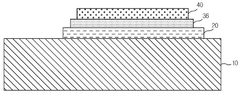
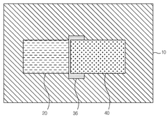
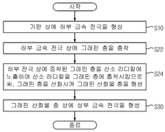
- The use of graphene oxide with insulating properties as the insulating layer in quantum devices, which can be formed to maintain a consistent and low thickness, compatible with existing semiconductor processes, thereby optimizing the thickness and quality of the insulating layer.
Nanoscale Manufacturing Considerations
Manufacturing at the nanoscale presents unique challenges when considering quantum tunneling effects on quasi-static device operations. The fabrication precision required to control tunneling phenomena demands extremely tight tolerances, typically in the sub-nanometer range. Current lithographic techniques, even advanced extreme ultraviolet (EUV) lithography with 5-7nm resolution, struggle to consistently produce structures where quantum effects are predictably managed rather than becoming operational liabilities.
Material selection becomes critically important at this scale. Traditional semiconductor materials exhibit different tunneling characteristics when dimensions approach the quantum regime. Silicon, for instance, demonstrates increased leakage current through thin gate oxides due to enhanced tunneling probability. Alternative materials such as high-k dielectrics and III-V semiconductors offer potential solutions by modifying the tunneling barrier height and width, though their integration introduces complex manufacturing considerations.
Process variability represents another significant manufacturing challenge. At nanoscale dimensions, even single-atom variations can dramatically alter tunneling probabilities. Statistical process control must evolve to account for quantum mechanical uncertainties, requiring new metrology approaches capable of characterizing quantum behavior during production rather than merely physical dimensions.
Temperature management during manufacturing becomes increasingly critical as quantum tunneling is temperature-dependent. Fabrication environments must maintain unprecedented temperature stability to ensure consistent tunneling characteristics across devices. This necessitates advanced thermal management systems throughout the manufacturing process, from material deposition to final testing.
Contamination control reaches new levels of importance when manufacturing devices where quantum tunneling is a significant operational factor. Even single molecules or atoms of contaminants can create localized changes in potential barriers, dramatically altering tunneling behavior. Clean room requirements may need to advance beyond current Class 1 standards to address quantum-level contamination concerns.
Testing and characterization methodologies must evolve to directly measure and verify quantum tunneling parameters during manufacturing. Traditional electrical testing becomes insufficient when quantum effects dominate device behavior. Novel in-line measurement techniques, potentially utilizing quantum probes themselves, may be necessary to ensure manufacturing consistency and product reliability in devices where tunneling effects are critical operational parameters.
Quantum Reliability and Stability Factors
Quantum reliability and stability factors represent critical considerations in the analysis of quantum tunneling effects on quasi-static device operations. The inherent probabilistic nature of quantum tunneling introduces significant challenges to maintaining consistent device performance over time. Reliability metrics must account for the stochastic behavior of electrons traversing potential barriers that classical physics would deem impenetrable.
Temperature fluctuations significantly impact quantum tunneling rates, with higher temperatures generally increasing tunneling probability through thermal excitation. This temperature dependence creates reliability concerns in environments with variable thermal conditions, necessitating robust compensation mechanisms. Device designers must implement temperature stabilization systems or adaptive algorithms that adjust operational parameters based on thermal feedback.
Voltage stability emerges as another crucial factor affecting quantum tunneling reliability. Even minor voltage fluctuations can dramatically alter the effective barrier height and width, leading to unpredictable changes in tunneling current. This sensitivity requires precision voltage regulation systems with tolerances significantly tighter than those in conventional electronic devices.
Material degradation over time presents a long-term stability challenge for quantum tunneling devices. Atomic-level defects, which may develop through normal operation or environmental exposure, can create localized changes in potential barrier characteristics. These changes may manifest as performance drift that becomes increasingly pronounced throughout the device lifecycle, complicating reliability predictions.
Statistical variance in tunneling behavior necessitates probabilistic reliability models rather than deterministic ones. Mean time between failure (MTBF) calculations must incorporate quantum uncertainty principles, resulting in reliability distributions rather than fixed values. This statistical approach requires more sophisticated quality assurance methodologies than those employed for classical devices.
Radiation hardness represents a particular concern for quantum tunneling devices deployed in aerospace, nuclear, or other high-radiation environments. Incident radiation can temporarily or permanently alter barrier characteristics, potentially causing catastrophic device failure or gradual performance degradation. Specialized shielding and redundancy architectures must be implemented to mitigate these effects.
The quantum coherence time of the system fundamentally limits operational stability in devices that leverage quantum state preservation. Environmental decoherence mechanisms, including electromagnetic interference and vibrational noise, can disrupt the quantum states necessary for reliable operation. Isolation techniques and error correction protocols become essential components of the reliability engineering approach for such devices.
Unlock deeper insights with PatSnap Eureka Quick Research — get a full tech report to explore trends and direct your research. Try now!
Generate Your Research Report Instantly with AI Agent
Supercharge your innovation with PatSnap Eureka AI Agent Platform!