

Chip Package Substrate Layer vs Solder Reliability: Case Metrics
APR 7, 20269 MIN READ
Generate Your Research Report Instantly with AI Agent
PatSnap Eureka helps you evaluate technical feasibility & market potential.
Chip Package Substrate Evolution and Reliability Goals
The evolution of chip package substrates has been fundamentally driven by the semiconductor industry's relentless pursuit of miniaturization, performance enhancement, and cost optimization. From the early ceramic substrates of the 1970s to today's advanced organic substrates with embedded components, this technological progression reflects the industry's response to Moore's Law and the increasing complexity of integrated circuits. The substrate serves as the critical interface between the silicon die and the printed circuit board, making its reliability paramount to overall system performance.
Modern substrate technology has evolved through several distinct phases, beginning with single-layer ceramic solutions and progressing to multi-layer organic substrates featuring fine-pitch interconnects and advanced materials. The transition from wire bonding to flip-chip packaging has fundamentally altered substrate design requirements, demanding higher interconnect density, improved thermal management, and enhanced electrical performance. This evolution has been accompanied by a corresponding shift in reliability challenges, particularly concerning solder joint integrity and substrate-level failures.
The primary reliability goals for contemporary chip package substrates center on achieving robust solder joint performance under various stress conditions including thermal cycling, mechanical shock, and long-term aging. Temperature cycling reliability remains the most critical metric, with industry standards typically requiring survival of 1000 to 3000 cycles between -40°C and 125°C without failure. The substrate must maintain structural integrity while accommodating the coefficient of thermal expansion mismatches between different materials in the package stack.
Electrical reliability objectives encompass maintaining signal integrity, minimizing crosstalk, and ensuring stable power delivery throughout the product lifecycle. As operating frequencies continue to increase and supply voltages decrease, substrates must demonstrate consistent dielectric properties and minimal conductor resistance drift over time. The reliability goals also extend to moisture resistance, with packages required to withstand multiple reflow cycles after moisture preconditioning according to JEDEC standards.
Mechanical reliability targets focus on preventing substrate cracking, delamination, and via failures under various loading conditions. The substrate must withstand assembly stresses, including die attach, wire bonding or flip-chip attachment, and subsequent board-level assembly processes. Long-term reliability goals encompass resistance to fatigue failure mechanisms, particularly in high-stress applications such as automotive and aerospace electronics where extended operational lifetimes are mandatory.
Market Demand for Advanced Packaging Solutions
The semiconductor industry is experiencing unprecedented demand for advanced packaging solutions, driven by the proliferation of high-performance computing applications, artificial intelligence processors, and mobile devices requiring enhanced functionality in compact form factors. This surge in demand directly correlates with the critical need for reliable chip package substrate and solder joint performance, as these components form the fundamental interconnection infrastructure supporting next-generation electronic systems.
Market drivers for advanced packaging technologies are primarily centered around the industry's transition toward heterogeneous integration and system-in-package architectures. Data centers and cloud computing infrastructure require processors with exceptional thermal management and electrical performance, necessitating sophisticated substrate materials and solder joint configurations that can withstand extreme operating conditions while maintaining signal integrity.
The automotive electronics sector represents another significant growth vector, particularly with the advancement of autonomous driving systems and electric vehicle powertrains. These applications demand packaging solutions with enhanced reliability metrics, as substrate layer delamination or solder joint failure can result in catastrophic system failures. Consequently, automotive manufacturers are increasingly specifying stringent reliability requirements for package substrates and interconnection materials.
Consumer electronics continue to push miniaturization boundaries while demanding increased functionality, creating substantial market pressure for advanced packaging solutions that optimize space utilization without compromising reliability. Smartphone manufacturers and wearable device producers require packaging technologies that can accommodate multiple die configurations while maintaining robust mechanical and thermal performance characteristics.
The telecommunications infrastructure market, particularly with the deployment of advanced wireless networks, requires packaging solutions capable of handling high-frequency signals with minimal loss while maintaining long-term reliability under varying environmental conditions. This application domain specifically emphasizes the importance of substrate material properties and solder joint integrity in maintaining network performance standards.
Emerging applications in aerospace and defense sectors are driving demand for packaging solutions with exceptional reliability under extreme environmental conditions, including temperature cycling, vibration, and radiation exposure. These markets require comprehensive understanding of substrate layer behavior and solder joint performance metrics to ensure mission-critical system reliability throughout extended operational lifecycles.
Current Substrate-Solder Interface Reliability Challenges
The substrate-solder interface in semiconductor packaging faces multiple reliability challenges that significantly impact device performance and longevity. Thermal cycling represents one of the most critical stress factors, where repeated expansion and contraction cycles create mechanical strain at the interface. The coefficient of thermal expansion mismatch between organic substrates and metallic solder materials generates substantial stress concentrations, particularly at bond pad edges and via connections.
Intermetallic compound formation poses another fundamental challenge affecting long-term reliability. During reflow processes and subsequent thermal exposure, copper from substrate traces reacts with tin-based solders to form Cu6Sn5 and Cu3Sn phases. While thin intermetallic layers provide adequate bonding, excessive growth creates brittle interfaces prone to crack initiation and propagation under mechanical stress.
Electromigration phenomena increasingly threaten interface integrity as current densities continue rising in advanced packaging architectures. High current flow through solder joints causes atomic migration, leading to void formation and eventual open circuits. This challenge becomes particularly acute in fine-pitch applications where individual solder volumes decrease while current requirements remain constant.
Moisture absorption by organic substrates introduces hygrothermal stress mechanisms that compromise interface adhesion. Absorbed moisture expands during thermal excursions, creating delamination forces at the substrate-solder boundary. This effect is amplified in lead-free solder systems that require higher processing temperatures, increasing moisture-driven stress levels.
Mechanical shock and vibration loading present additional reliability concerns, especially in automotive and aerospace applications. Dynamic loading conditions can exceed the fatigue limits of solder joints, particularly when combined with thermal cycling effects. The substrate's mechanical properties, including flexural strength and elastic modulus, directly influence stress distribution and crack propagation rates.
Surface contamination and oxidation issues further complicate reliability assessment. Organic residues, flux remnants, and native oxide layers can prevent proper metallurgical bonding, creating weak interfaces susceptible to early failure. Advanced surface preparation and cleaning protocols become essential for achieving consistent interface quality and long-term reliability performance in demanding applications.
Current Substrate-Solder Reliability Testing Methods
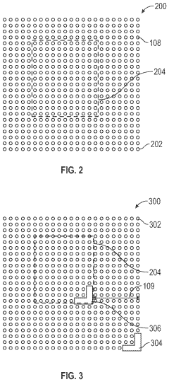
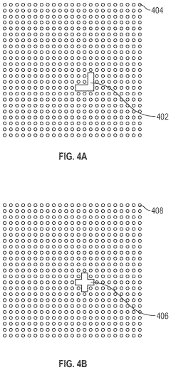
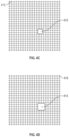
01 Solder bump structure and formation methods
Various solder bump structures and their formation methods are designed to enhance reliability in chip package substrates. These include optimized bump geometries, multi-layer bump structures, and controlled solder composition to improve mechanical strength and thermal cycling performance. The formation processes involve precise control of plating, reflow, and underfill techniques to ensure robust solder joints that can withstand stress during operation and assembly.- Solder bump structure and formation methods: Various solder bump structures and formation methods are employed to enhance the reliability of chip package substrates. These include optimized bump geometries, multi-layer solder compositions, and controlled reflow processes. The structures are designed to improve mechanical strength, reduce stress concentration, and enhance electrical connectivity. Advanced bump formation techniques such as electroplating, stencil printing, and ball placement are utilized to achieve uniform solder distribution and proper adhesion to substrate pads.
- Underfill materials and encapsulation techniques: Underfill materials are applied between the chip and substrate to improve solder joint reliability by redistributing thermal and mechanical stresses. These materials typically consist of epoxy resins with specific thermal expansion coefficients and flow characteristics. The encapsulation process fills the gap between components, providing mechanical support and protection against environmental factors. Various dispensing methods and curing processes are optimized to ensure complete filling without voids or delamination.
- Substrate material composition and layer structure: The substrate material composition and multilayer structure significantly impact solder joint reliability. Advanced substrates utilize materials with controlled thermal expansion coefficients to match chip and solder properties. Layer configurations include core materials, dielectric layers, and copper circuitry designed to minimize warpage and stress during thermal cycling. Material selection considers factors such as glass transition temperature, moisture absorption, and dimensional stability to ensure long-term reliability.
- Thermal management and stress reduction designs: Thermal management structures and stress reduction designs are incorporated to enhance solder reliability under operating conditions. These include heat spreaders, thermal vias, and optimized pad layouts that distribute heat and mechanical stress more evenly. Design features such as compliant layers, stress buffer zones, and controlled coefficient of thermal expansion matching help accommodate differential expansion between materials. These approaches minimize fatigue and cracking in solder joints during temperature cycling.
- Testing and reliability assessment methods: Comprehensive testing and reliability assessment methods are employed to evaluate solder joint performance in chip package substrates. These include thermal cycling tests, mechanical shock testing, and accelerated aging protocols that simulate real-world operating conditions. Non-destructive testing techniques such as X-ray inspection and acoustic microscopy detect defects and voids. Reliability metrics are established through statistical analysis of failure modes, enabling prediction of product lifetime and optimization of manufacturing processes.
02 Underfill materials and encapsulation techniques
Underfill materials are applied between the chip and substrate to redistribute stress and protect solder joints from mechanical and thermal fatigue. Advanced encapsulation techniques involve the use of specialized polymeric materials with controlled flow properties and curing characteristics. These materials fill the gaps around solder bumps, providing mechanical support and preventing crack propagation, thereby significantly improving the overall reliability of the package assembly.Expand Specific Solutions03 Substrate material composition and layer structure
The substrate material composition and multilayer structure play critical roles in solder joint reliability. Advanced substrates utilize materials with matched thermal expansion coefficients to reduce stress at solder interfaces. Layer structures are optimized with appropriate dielectric materials, copper thickness, and via designs to enhance electrical performance while maintaining mechanical integrity. These design considerations help minimize warpage and improve the long-term reliability of solder connections.Expand Specific Solutions04 Thermal management and stress reduction designs
Thermal management structures and stress reduction designs are incorporated into package substrates to improve solder reliability. These include heat spreaders, thermal vias, and optimized pad designs that distribute heat more evenly and reduce thermal gradients. Stress buffer layers and compliant structures are also employed to absorb mechanical stress caused by coefficient of thermal expansion mismatches, preventing solder joint fatigue and cracking during temperature cycling.Expand Specific Solutions05 Testing and reliability assessment methods
Comprehensive testing and reliability assessment methods are essential for evaluating solder joint performance in chip package substrates. These methods include accelerated thermal cycling tests, mechanical shock and vibration testing, and electrical continuity monitoring. Advanced inspection techniques such as X-ray imaging and acoustic microscopy are used to detect voids, cracks, and delamination. Reliability models and failure analysis help predict service life and identify potential failure modes for design optimization.Expand Specific Solutions
Major Players in Semiconductor Packaging Industry
The chip package substrate layer versus solder reliability research represents a critical technology area within the mature semiconductor packaging industry, which has reached a market size exceeding $30 billion globally. The competitive landscape is dominated by established players across different segments of the value chain. Leading foundries like Taiwan Semiconductor Manufacturing Co. and Samsung Electronics drive advanced packaging innovations, while specialized assembly and test service providers including JCET Group, Siliconware Precision Industries, and TongFu Microelectronics focus on reliability optimization. Memory manufacturers such as SK hynix, Micron Technology, and ChangXin Memory Technologies contribute substrate-related innovations for their high-density products. The technology maturity varies significantly, with companies like Intel and Texas Instruments leading in advanced substrate materials research, while emerging players like China Wafer Level CSP and Huatian Technology are rapidly developing competitive capabilities in specialized packaging solutions.
Samsung Electronics Co., Ltd.
Technical Solution: Samsung has developed advanced package substrate technologies focusing on multi-layer organic substrates with enhanced thermal and electrical performance. Their approach integrates fine-pitch interconnects with optimized solder joint reliability through controlled via structures and copper trace geometries. The company employs advanced materials including low-loss dielectrics and high-density interconnect (HDI) technologies to achieve superior signal integrity while maintaining mechanical robustness. Samsung's substrate solutions feature embedded passive components and optimized layer stackups that reduce parasitic effects and improve overall package reliability under thermal cycling and mechanical stress conditions.
Strengths: Leading-edge manufacturing capabilities, extensive R&D resources, integrated supply chain control. Weaknesses: High development costs, complex manufacturing processes requiring specialized equipment.
Amkor Technology Singapore Holding Pte Ltd.
Technical Solution: Amkor has developed specialized substrate reliability assessment methodologies focusing on their System-in-Package (SiP) and flip-chip Ball Grid Array (fcBGA) solutions. Their approach integrates comprehensive solder joint reliability testing with substrate layer optimization, employing advanced finite element modeling to predict failure modes under various stress conditions. Amkor's substrate technologies feature optimized copper pillar and solder cap configurations that enhance mechanical reliability while reducing electrical resistance. The company has established standardized reliability metrics including board-level reliability (BLR) testing protocols and has developed proprietary underfill materials that improve solder joint fatigue resistance in automotive and industrial applications requiring extended operational lifetimes.
Strengths: Extensive packaging expertise, strong automotive qualification capabilities, comprehensive reliability testing facilities. Weaknesses: Limited substrate manufacturing capabilities, dependence on external substrate suppliers for advanced technologies.
Key Innovations in Substrate-Solder Interface Design
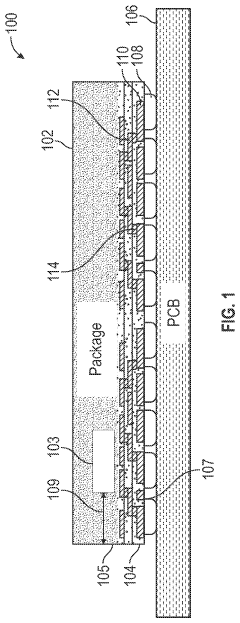
Semiconductor package
PatentInactiveUS20120049368A1
Innovation
- A semiconductor package design incorporating through-silicon vias with a base material having a linear expansion coefficient of 3 to 8 ppm/°C, which minimizes electrical connection length and parasitic capacitance, and uses micro vias and ceramic materials to suppress warpage and enhance connection reliability.


Solder joint design for improved package reliability
PatentPendingUS20240063141A1
Innovation
- Incorporating additional solder joints of varying shapes and sizes at strategic locations on the semiconductor package, which act as mechanical supports and increase the interfacial area with bonding pads, thereby enhancing mechanical strength and reliability.
Industry Standards for Package Reliability Testing
The semiconductor packaging industry relies on a comprehensive framework of standardized testing protocols to evaluate package reliability, particularly for substrate layer and solder joint performance assessment. These standards provide essential benchmarks for measuring reliability metrics and ensuring consistent evaluation methodologies across different manufacturers and applications.
JEDEC Solid State Technology Association serves as the primary governing body for semiconductor reliability standards, establishing critical testing protocols such as JESD22 series specifications. These standards define accelerated stress testing conditions including thermal cycling, temperature humidity bias, and highly accelerated stress testing that directly impact substrate-solder interface reliability evaluation.
IPC standards, particularly IPC-9701 series, focus specifically on performance characterization of electronic assemblies under various environmental conditions. These specifications establish standardized test vehicles and measurement techniques for evaluating solder joint reliability in advanced packaging configurations, providing crucial guidance for substrate layer interaction studies.
International standards organizations including ISO and IEC contribute additional frameworks for reliability assessment methodologies. ISO 16750 automotive electronics standards and IEC 60749 semiconductor device reliability testing standards offer complementary approaches to package reliability evaluation, particularly relevant for high-reliability applications where substrate-solder performance is critical.
Military and aerospace standards such as MIL-STD-883 and RTCA DO-160 establish more stringent reliability requirements and testing protocols. These standards often require extended testing durations and more severe stress conditions, providing valuable insights into long-term substrate layer and solder joint degradation mechanisms under extreme operating environments.
Industry consortiums including SEMI and ECTC continuously develop emerging standards addressing advanced packaging technologies. These evolving standards incorporate new testing methodologies for 3D packaging, system-in-package configurations, and heterogeneous integration approaches where substrate layer complexity significantly impacts overall reliability performance.
The standardization landscape continues evolving to address emerging challenges in package miniaturization, increased power density, and multi-layer substrate configurations. Recent standard updates emphasize statistical analysis requirements and failure mode characterization protocols essential for comprehensive reliability case metric development.
Thermal Management Impact on Substrate Reliability
Thermal management plays a critical role in determining substrate reliability within chip package assemblies, as temperature fluctuations and thermal gradients directly influence the mechanical integrity of substrate materials and their interconnection systems. The substrate, typically composed of organic materials such as BT resin or polyimide, exhibits temperature-dependent mechanical properties that significantly affect its long-term performance under operational conditions.
During thermal cycling, the coefficient of thermal expansion (CTE) mismatch between the substrate layers and adjacent components creates mechanical stress concentrations. The substrate's organic dielectric materials typically have CTE values ranging from 15-20 ppm/°C, which differs substantially from silicon (2.6 ppm/°C) and copper traces (17 ppm/°C). This mismatch generates cyclic stress patterns that can lead to delamination, cracking, and via failure within the substrate structure.
Elevated operating temperatures accelerate chemical degradation processes within substrate materials, including polymer chain scission, oxidation, and moisture absorption. These phenomena reduce the substrate's mechanical strength and dimensional stability over time. Research indicates that substrate reliability follows an Arrhenius relationship, where every 10°C temperature increase can potentially halve the operational lifetime of organic substrate materials.
Thermal gradients across the substrate surface create non-uniform expansion patterns that induce warpage and mechanical distortion. This warpage directly impacts the planarity requirements for solder joint formation and can compromise the reliability of ball grid array (BGA) and land grid array (LGA) connections. The substrate's ability to maintain dimensional stability under thermal stress becomes crucial for preventing solder joint fatigue and ensuring long-term electrical connectivity.
Heat dissipation efficiency through the substrate also influences local temperature distributions around critical solder joints. Poor thermal management can create hotspots that accelerate intermetallic compound growth at solder interfaces, leading to brittle joint formation and reduced mechanical reliability. The substrate's thermal conductivity, typically ranging from 0.3-0.8 W/mK for organic materials, becomes a limiting factor in overall thermal performance.
Advanced thermal management strategies, including embedded thermal vias, heat spreaders, and optimized copper plane designs, are essential for maintaining substrate reliability under high-power applications. These approaches help minimize temperature gradients and reduce peak operating temperatures, thereby extending substrate operational lifetime and maintaining mechanical integrity throughout the product lifecycle.
Unlock deeper insights with PatSnap Eureka Quick Research — get a full tech report to explore trends and direct your research. Try now!
Generate Your Research Report Instantly with AI Agent
Supercharge your innovation with PatSnap Eureka AI Agent Platform!