
Electrophoretic display and manufacturing method thereof
An electrophoretic display, electrophoretic display technology, applied in instruments, nonlinear optics, optics, etc., to avoid damage, reduce damage, and improve the yield of the manufacturing process
Patent Information
- Authority / Receiving Office
- CN · China
- Patent Type
- Applications(China)
- Current Assignee / Owner
- Publication Date
- 2011-06-29
Smart Images
Figure 1 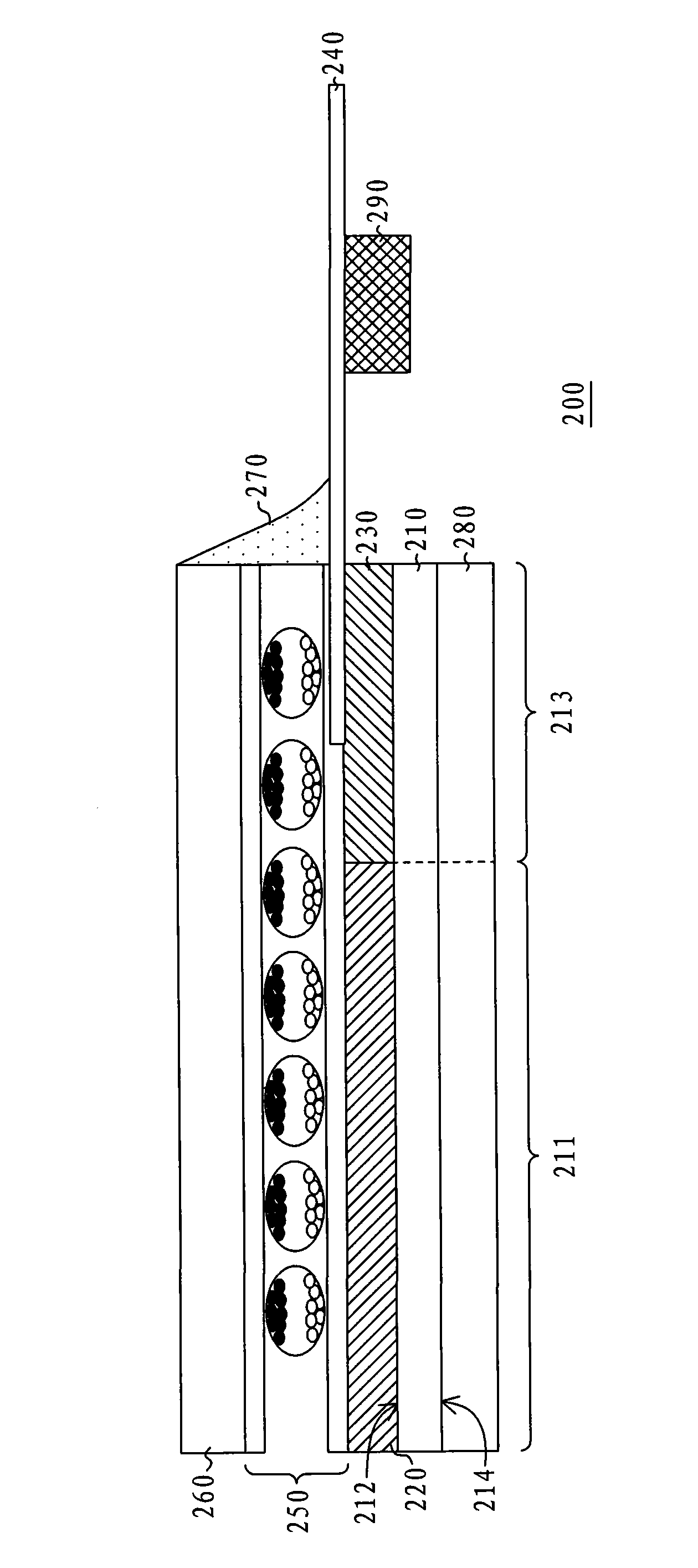
Figure 2 
Figure 3
Abstract
Description
technical field
[0001] The invention relates to a display and a manufacturing method thereof, in particular to an electrophoretic display and a manufacturing method thereof. Background technique
[0002] With the advancement of flat panel display technology, more and more electronic products are equipped with displays, especially portable electrical products, such as mobile phones, e-books, digital Camera (digital camera) and personal digital assistant (personal digital assistant, PDA), etc. Since portable electronic products tend to be light in weight and thin in thickness, displays used in portable electronic products also need to have the advantages of light in weight and thin in thickness.
[0003] Based on the above, since flexible displays not only have the advantages of light weight and thin thickness, but also have the advantages of being flexible and unbreakable, the manufacture of flexible displays has become an important development trend. At present, the common...
Examples
Embodiment Construction
[0058] In order to further explain the technical means and effects of the present invention to achieve the intended purpose of the invention, below in conjunction with the accompanying drawings and preferred embodiments, the specific implementation, structure, method, Steps, features and effects thereof are described in detail below.
[0059] figure 2 It is a partial cross-sectional schematic diagram of an electrophoretic display in an embodiment of the present invention. Please refer to figure 2 As shown, the electrophoretic display 200 includes a first substrate 210 , an active element array 220 , a driving circuit 230 , a conductive flexible plate 240 , an electrophoretic display layer 250 , a second substrate 260 and a sealant 270 . Wherein, the first substrate 210 has a first surface 212 , and the first surface 212 has a display area 211 and a circuit area 213 . The first substrate 210 of this embodiment may be a flexible substrate made of plastic materials. Specific...