
Packaging structure for light emitting diode light source
A technology of light-emitting diodes and packaging structures, applied in the direction of electric solid-state devices, semiconductor devices, electrical components, etc., can solve the problems of low voltage efficiency and current fluctuations, achieve short circuit connections, increase life, and save coating costs Effect
Patent Information
- Authority / Receiving Office
- CN · China
- Patent Type
- Patents(China)
- Current Assignee / Owner
- Publication Date
- 2012-09-26
- Estimated Expiration
- Not applicable · inactive patent
Smart Images
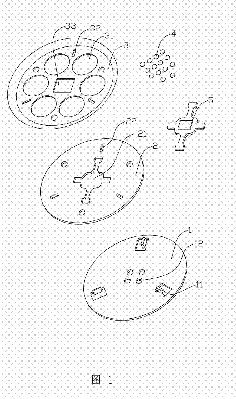
Figure 1 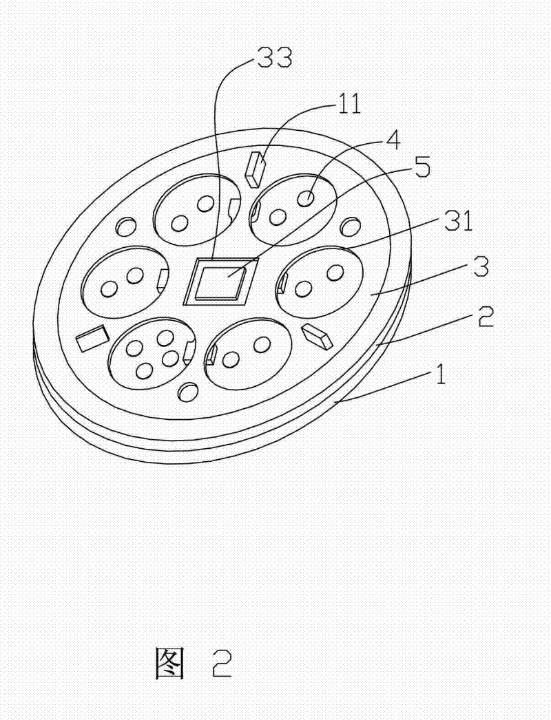
Figure 2 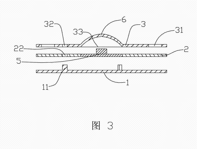
Figure 3
Abstract
Description
technical field
[0001] The invention relates to the field of lighting equipment, and more specifically refers to a packaging structure of a light emitting diode light source. Background technique
[0002] At present, the light-emitting diode light source and the power driver are mostly separated, and some of them are driven by low-voltage DC power supply. The power supply below 8 watts has a low power supply efficiency, which is about 85% or less, and the power factor is also low, about 0.85 or less. ; Some parts use high-voltage AC LEDs, and their AC power is directly connected to multiple strings of LEDs, but due to changes in their voltage, it is easy to cause current fluctuations; some use electrolytic capacitors to step down and stabilize the current, but their power supply Factors are generally below 0.5, resulting in waste of grid power supply. Contents of the invention
[0003] The present invention provides a package structure of a light emitting diode light sour...
Examples
Embodiment 1
[0026] Such as figure 1 , figure 2 As shown, a package structure of a light-emitting diode light source includes a first stamped metal sheet 1, a second stamped metal sheet 2, and a third stamped metal sheet 3 in a circular structure, which are attached to the second stamped metal sheet 2. The light-emitting diode chip 4, the PCB circuit board 5 connected with the light-emitting diode chip 4, the second stamping metal sheet 2 is provided with the installation port 21 that can fix the PCB circuit board 5, and the third stamping metal sheet 3 is provided with There are six openings 31 that limit the areas of fluorescent powder glue, and the above-mentioned light-emitting diode chips 4 are attached to the six areas of the second punched metal sheet 2 corresponding to the through holes 31; the second punched metal sheet 2 is along the The second stamped metal sheet 2 is evenly arranged with three bayonet sockets 22 on the circumference, and the third stamped metal sheet 3 is eve...
Embodiment 2
[0032] This embodiment is roughly the same as Embodiment 1, as image 3 , Figure 4 As shown, only a convex portion 6 is provided at the position of the limit opening 33 of the third punched metal sheet 3, the convex portion 6 is conical or arc-shaped, and the convex portion 6 can cover the PCB circuit board 5 to avoid The light is absorbed by the PCB circuit board 5 .