
A kind of igbt chip variable gate internal resistance and its design method
A design method and technology of gate internal resistance, applied in electrical components, circuits, semiconductor devices, etc., can solve problems such as affecting the current and voltage of IGBT chips, fixed resistance, etc., to achieve easy implementation, strong feasibility, and improved fixed gate resistance. The effect of the defect of the value
Patent Information
- Authority / Receiving Office
- CN · China
- Patent Type
- Patents(China)
- Current Assignee / Owner
- Publication Date
- 2016-04-20
Smart Images
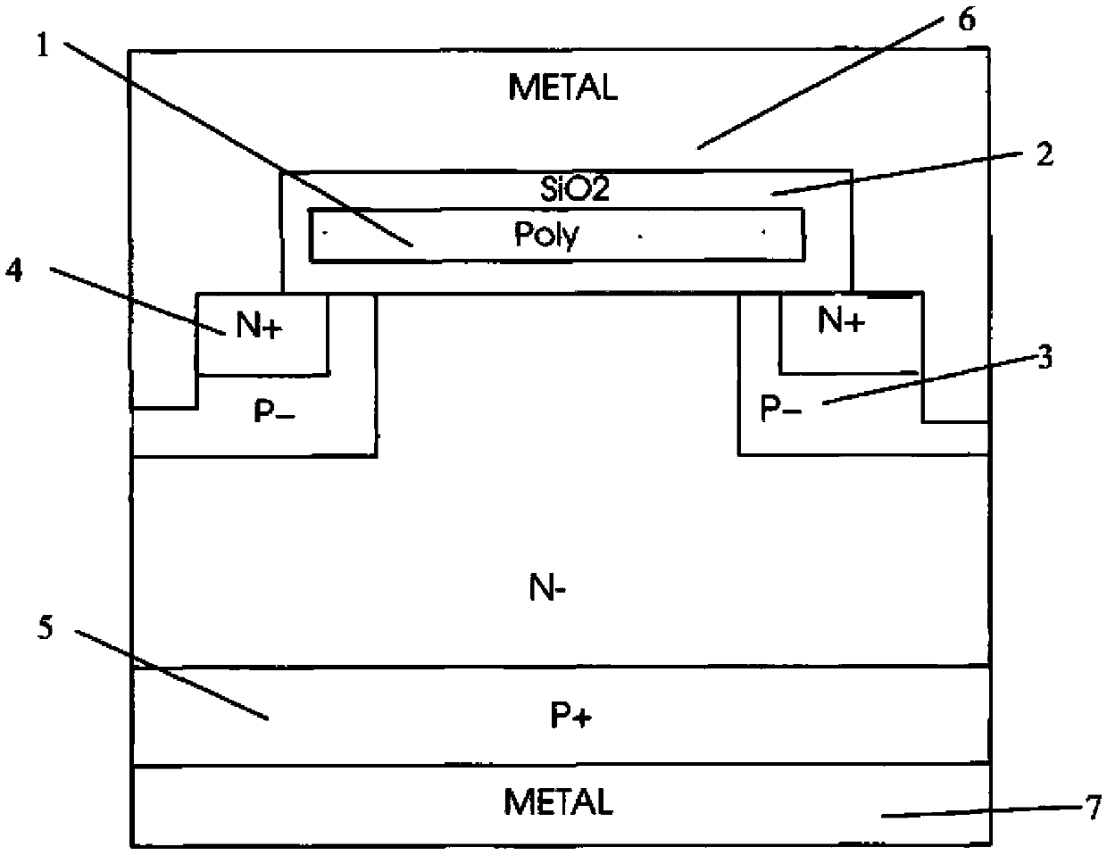
Figure 1 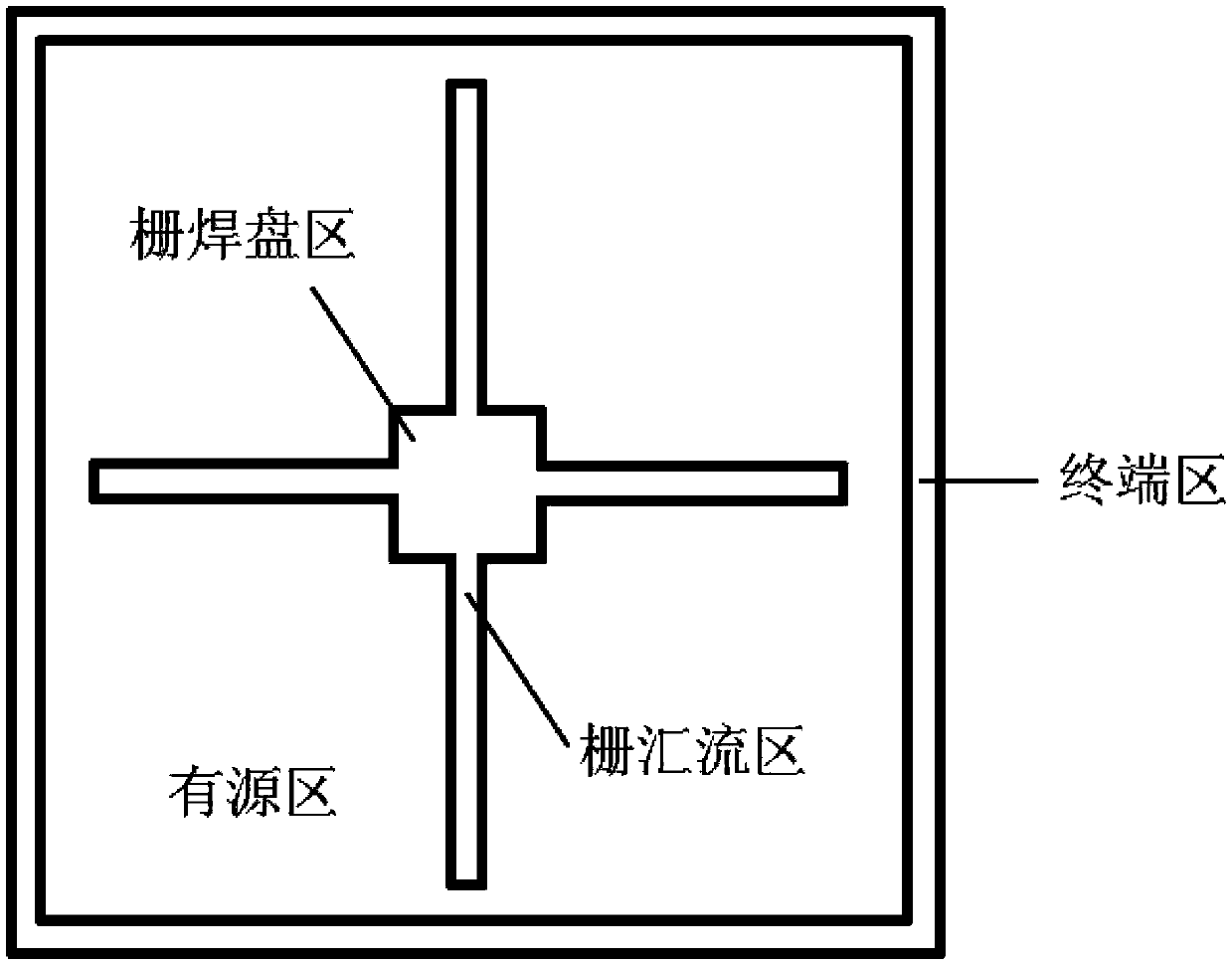
Figure 2 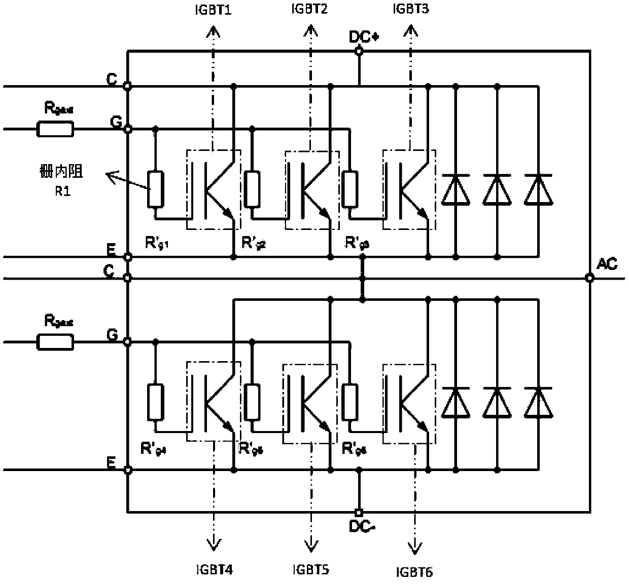
Figure 3
Abstract
Description
technical field
[0001] The invention relates to a gate internal resistance and a manufacturing method thereof, in particular to an IGBT chip variable gate internal resistance and a design method thereof. Background technique
[0002] IGBT (Insulated Gate Bipolar Transistor) has the advantages of both unipolar devices and bipolar devices, simple driving circuit, low power consumption and cost of control circuit, low on-state voltage, and low loss of the device itself. It is the future choice for high voltage and high current. Direction of development.
[0003] The IGBT is a 3-terminal device, including a front emitter, a gate and a back collector. For the cross-sectional view of the active area of the IGBT chip, see figure 1 . Including a low-concentration N-substrate region; a gate oxide layer 2 on the substrate surface, a polysilicon gate 1 deposited on the gate oxide layer 2; a P-well between the gate oxide layer and the N-substrate region Region 3; N+ region 4 betwe...
Examples
Embodiment Construction
[0047] The schematic diagram of IGBT parallel gate internal resistance is as follows image 3 As shown in the figure, IGBT1, IGBT2 and IGBT3 are connected in parallel, IGBT4, IGBT5 and IGBT6 are connected in parallel, and the gate internal resistance R’ g1 In series with IGBT1 chip, R’ g2 In series with IGBT2; R' g3 In series with IGBT3; R' g4 In series with IGBT4; R' g5 In series with IGBT5; R' g6 Connect in series with IGBT6.
[0048] The schematic diagram of the internal resistance of the gate of the IGBT chip is as follows: Figure 5 As shown, the design of the gate area of the IGBT chip usually also designs the gate resistance, which is called the gate internal resistance. The gate area of the IGBT chip includes the gate pad area and the gate bus bar area; the gate area commonly used in the IGBT chip has a planar type and a trench type. When IGBT chips are used in series, a resistor of about 2-10Ω (ohm) is usually connected in series between the gate pad area a...