
Electronic package and fabrication method thereof
A technology for electronic packages and electronic components, which is applied in the manufacture of electrical components, electric solid devices, semiconductor/solid devices, etc., and can solve the problem of increasing the volume of semiconductor packages 1, increasing the surface area of substrates 10, and not conforming to the lightness and thinness of semiconductor packages. issues such as short development trends
Patent Information
- Authority / Receiving Office
- CN · China
- Patent Type
- Applications(China)
- Current Assignee / Owner
- Publication Date
- 2017-02-15
- Estimated Expiration
- Not applicable · inactive patent
Smart Images
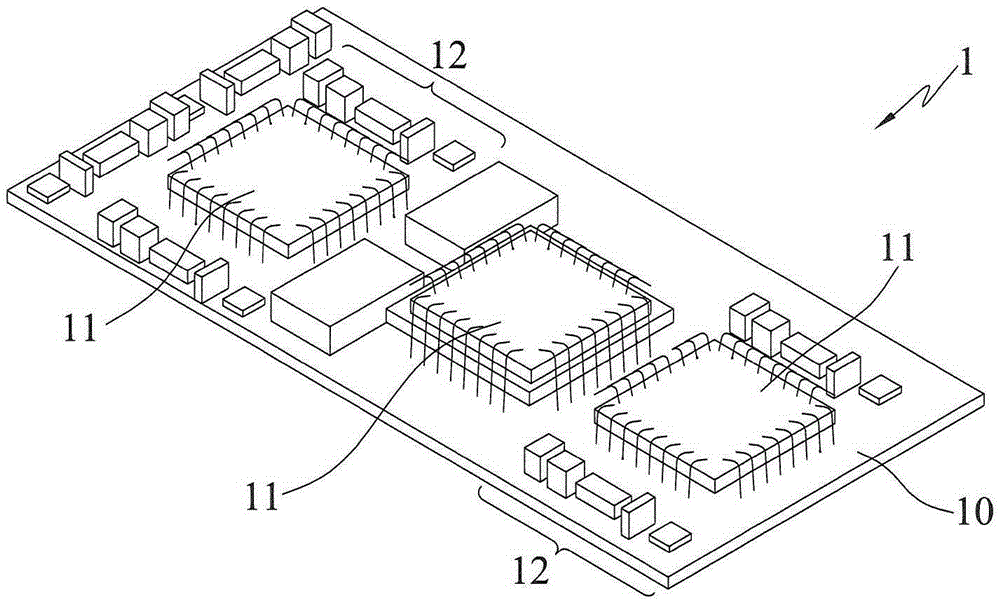
Figure 1 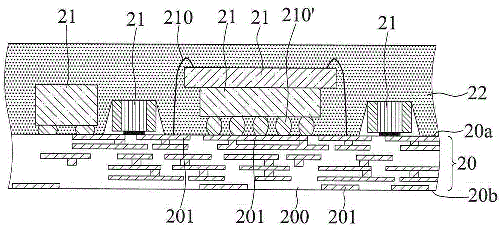
Figure 2 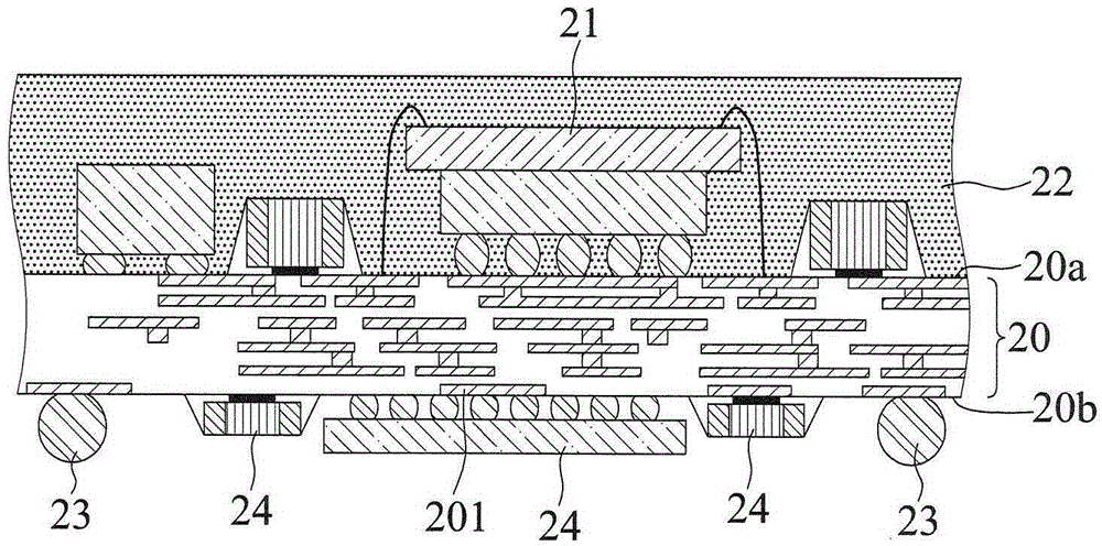
Figure 3
Abstract
Description
technical field
[0001] The invention relates to an electronic package, in particular to an electronic package with lightness, thinness and miniaturization and its manufacturing method. Background technique
[0002] Due to the vigorous development of the electronic industry, most electronic products are developing toward the goal of miniaturization and high speed, especially the development of the communication industry has been widely used in various electronic products, such as mobile phones (Cell phone), laptop Type computer (laptop) and so on.
[0003] At present, due to the miniaturization of electronic products and the increase in the demand for high operating speed, in order to improve the performance and capacity of a single semiconductor package to meet the needs of miniaturization of electronic products, the semiconductor package adopts multi-chip modularization (Multichip Module) It has become a trend to combine two or more chips in a single package to reduce the ...
Examples
Embodiment Construction
[0043] The implementation of the present invention is described below through specific specific examples, and those skilled in the art can easily understand other advantages and effects of the present invention from the content disclosed in this specification.
[0044] It should be noted that the structures, proportions, sizes, etc. shown in the drawings of this specification are only used to match the content disclosed in the specification for the understanding and reading of those skilled in the art, and are not used to limit the conditions for the implementation of the present invention , so it has no technical substantive meaning, and any modification of structure, change of proportional relationship or adjustment of size shall still fall within the scope of the disclosure of the present invention without affecting the functions and objectives of the present invention. The technical content must be within the scope covered. At the same time, terms such as "above", "first",...