
Electric connector
A technology for electrical connectors and electrical connections, applied in connection, fixed connections, circuits, etc., can solve problems affecting the production efficiency of electrical connectors, achieve simple structure, reduce manufacturing costs and difficulties, and simplify the manufacturing process.
Patent Information
- Authority / Receiving Office
- CN · China
- Current Assignee / Owner
- Publication Date
- 2017-08-25
- Estimated Expiration
- Not applicable · inactive patent
Smart Images
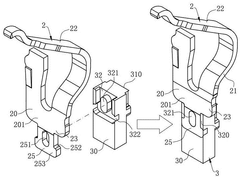
Figure 1 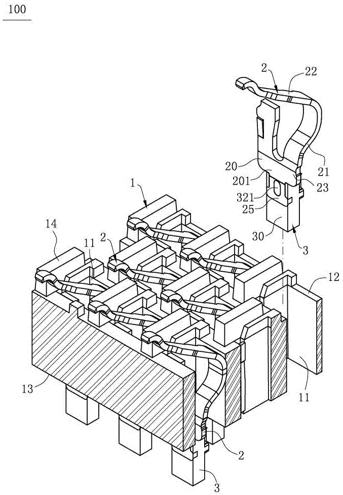
Figure 2 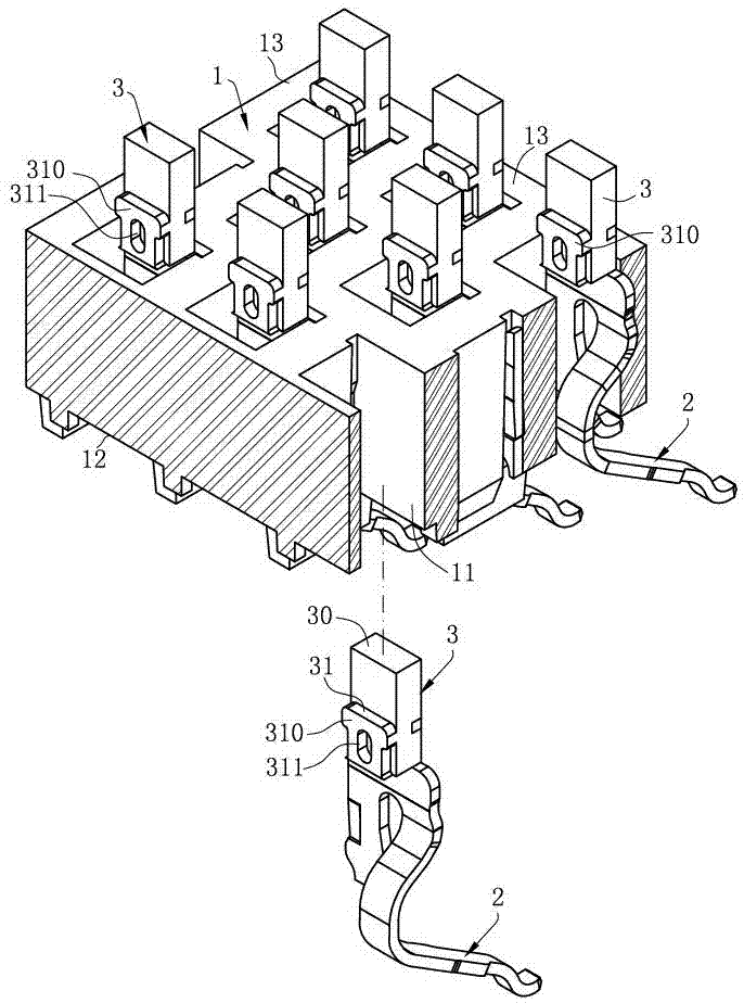
Figure 3
Abstract
Description
technical field
[0001] The invention relates to an electrical connector, in particular to an electrical connector in which the solder is fixed to a terminal by extruding the solder with a jig. Background technique
[0002] A conventional electrical connector includes a body with a plurality of receiving holes, and a plurality of terminals fixed in the plurality of receiving holes, and a plurality of solder balls are fixed to the terminals by heating and welding. However, in order to solder the solder balls on the terminals, they must go through the tin furnace for heating, which requires the equipment for positioning the solder balls and the equipment for transporting the electrical connector through the tin furnace, thus affecting the production efficiency of the electrical connector.
[0003] Therefore, it is necessary to design a new electrical connector to overcome the above problems. Contents of the invention
[0004] In view of the problems faced by the background t...
Examples
Embodiment Construction
[0031] In order to facilitate a better understanding of the purpose, structure, features, and effects of the present invention, the present invention will now be further described in conjunction with the accompanying drawings and specific embodiments.
[0032] Such as Figure 1 to Figure 5 Shown is the first embodiment of the electrical connector 100 of the present invention, which is used to electrically connect a chip module 200 to a circuit board 300, including an insulating body 1; a plurality of terminals 2 accommodated in the insulating body 1; a plurality of Solder 3, each of the solder 3 is fixed to the terminal 2 respectively.
[0033] Such as figure 2 with image 3 As shown, the insulating body 1 has an upper surface 12 and a lower surface 13 which are arranged oppositely, and the insulating body 1 has a plurality of through holes 11 which are arranged in a row and are dislocated, passing through the upper surface 12 and the lower surface 13, and the upper surface...