
Probe card
A technology of probe cards and probes, which is applied in the field of probe cards, can solve problems such as low position accuracy of the front end of probes, decreased strength of guide plates for probe cards, wrong measurement of probe cards, etc., and achieve effective aging testing The effect of manufacturing process, realizing narrow spacing, and effective heat dissipation
Patent Information
- Authority / Receiving Office
- CN · China
- Patent Type
- Applications(China)
- Current Assignee / Owner
- Publication Date
- 2021-04-06
Smart Images
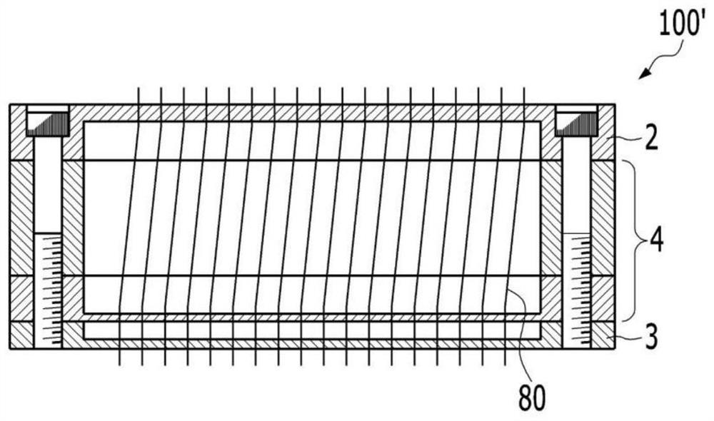
Figure 1 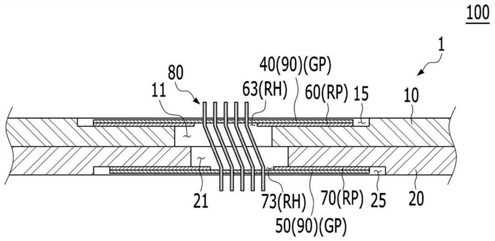
Figure 2 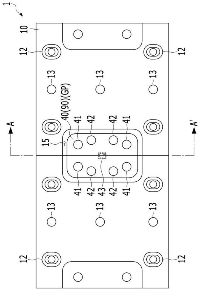
Figure 3
Abstract
Description
technical field
[0001] The present invention relates to a probe card for inspecting a pattern formed on a wafer. Background technique
[0002] The electrical characteristic test of a semiconductor element is performed by bringing a semiconductor wafer close to a probe card having a plurality of probes formed on a wiring board, and bringing each probe into contact with a corresponding electrode pad on the semiconductor wafer. After the probes reach the positions where they come into contact with the electrode pads, the semiconductor wafer can be raised further toward the probe card side by a certain height. The process as described above is called overpressurization, and the distance by which the wafer is further raised by a specific height is called overpressurization amount.
[0003] Overpressure can be the process of elastically deforming the probe. Even if the height of the electrode pads or the height of the probes varies due to overvoltage, all the probes can be relia...
Examples
Embodiment Construction
[0090] The following merely illustrates the principles of the invention. Therefore, although not explicitly described or illustrated in this specification, those skilled in the art can realize the principle of the invention and invent various devices included in the concept and scope of the invention. In addition, it should be understood that all conditional terms and examples listed in this specification are only for clearly understanding the concept of the invention in principle, and are not limited to such specifically listed examples and states.
[0091] The above objects, features, and advantages will be clarified by the following detailed description related to the accompanying drawings, so those skilled in the art to which the invention pertains can easily implement the technical idea of the invention.
[0092] Embodiments described in this specification are described with reference to cross-sectional views and / or perspective views which are ideal illustrations of the...