
Multilayer wiring board assembly, multilayer wiring board assembly component and method of manufacture thereof
a multi-layer wiring board and assembly technology, applied in the direction of etching metal masks, printed element electric connection formation, insulating substrate metal adhesion improvement, etc., can solve the problem of excessive occupied area of interlayer interconnection, essentially very difficult to assemble a plurality of fpcs in a multi-layered structure, and inability to form a new via hole on another via hole, etc., to achieve good heat resistance
Patent Information
- Authority / Receiving Office
- US · United States
- Current Assignee / Owner
- Publication Date
- 2005-01-27
- Estimated Expiration
- Not applicable · inactive patent
Smart Images
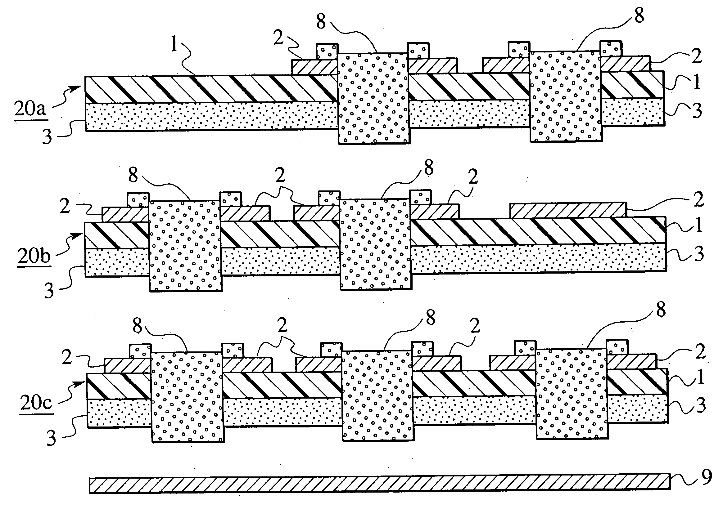
Figure 1 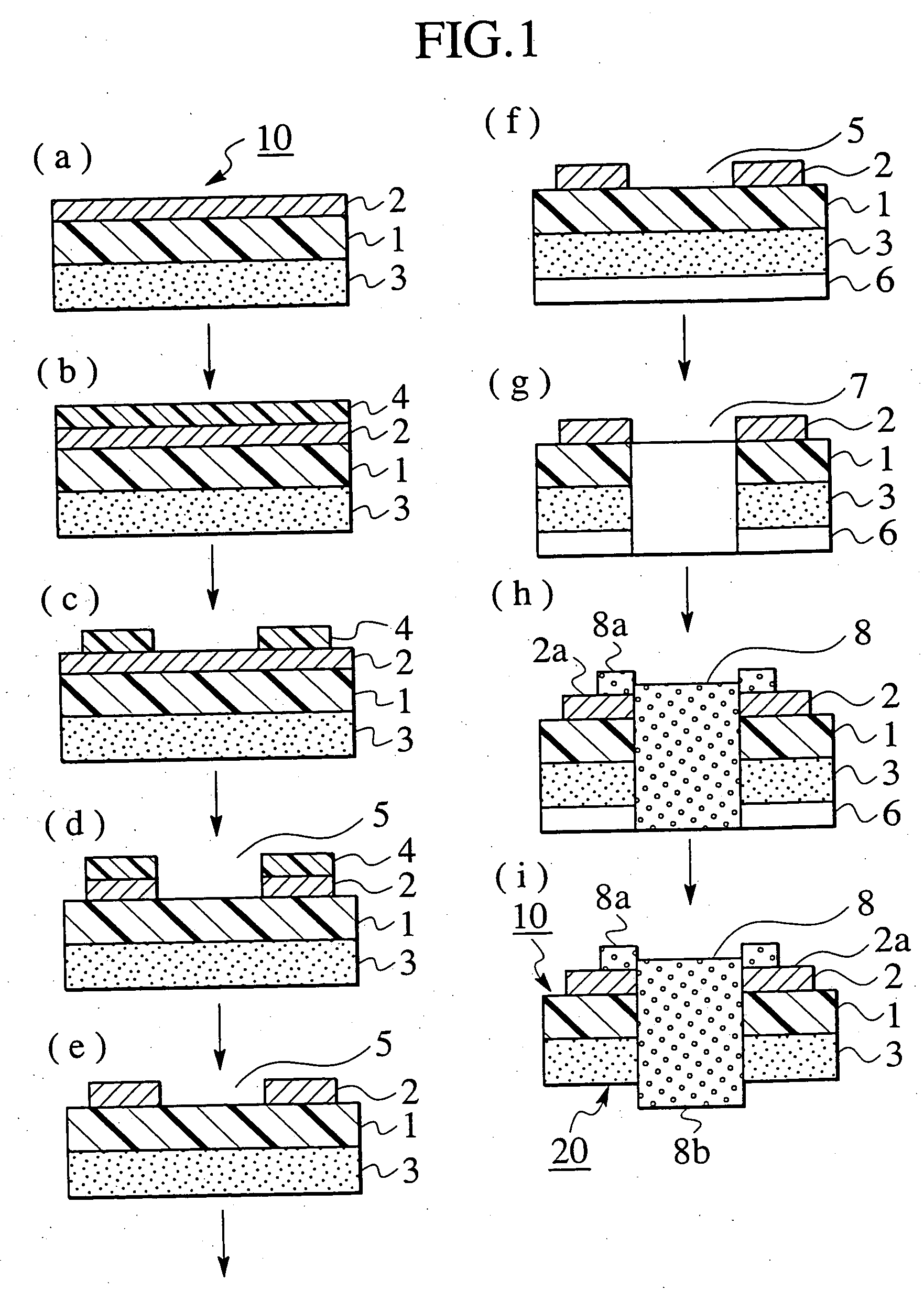
Figure 2 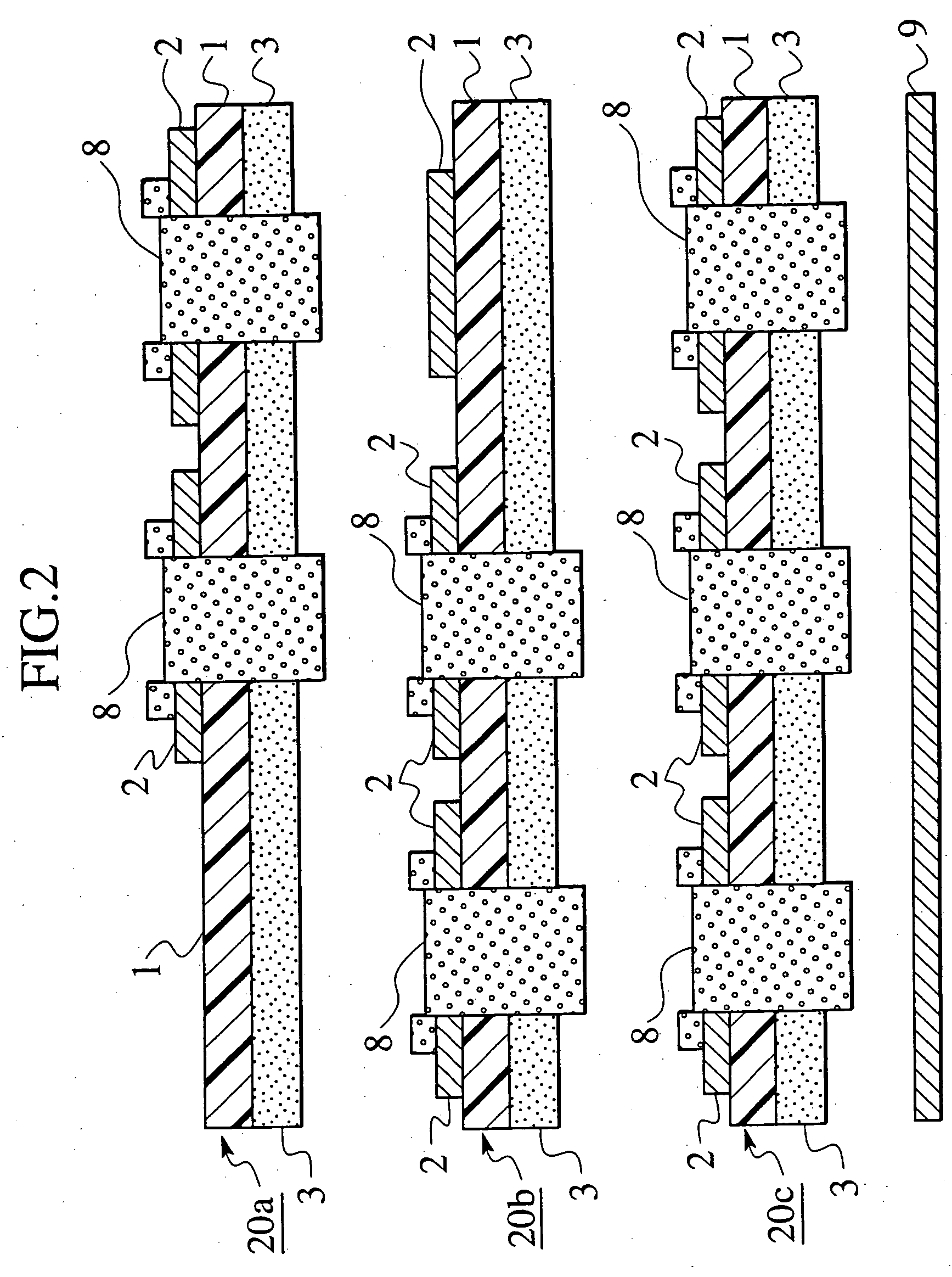
Figure 3
Abstract
Description
CROSS REFERENCE TO RELATED APPLICATIONS
[0001] This application is based upon and claims the benefit of priority from prior Japanese Patent Applications P2001-85224 filed on Mar. 23rd, 2001; P2002-76334 filed on Mar. 19rd, 2002; P2002-76335 filed on Mar. 19rd, 2002; P2002-76226 filed on Mar. 19rd, 2002; P2002-76523 filed on Mar. 19rd, 2002; the entire contents of which are incorporated by reference herein. BACKGROUN OF THE INVENTION
[0002] 1. Field of the Invention
[0003] The present invention relates to a multilayer wiring board assembly composed of a plurality of printed circuit boards in a multilayered structure, a multilayer wiring board assembly component for use in laminating the same and the manufacturing method of the same. In particular, the present invention relates to a multilayer wiring board assembly, a multilayer wiring board assembly component for use in laminating the same and the manufacturing method of the same, wherein the multilayer wiring board assembly is flexi...
Examples
Embodiment Construction
[0080] In the followings, various preferred embodiments of the present invention will be described with reference to the accompanying drawings.
[0081]FIG. 1 shows cross sectional views of the intermediate structures of a multilayer wiring board assembly component for use in manufacturing a multilayer wiring board assembly in accordance with an embodiment of the present invention in the order of the manufacturing steps. FIG. 2 and FIG. 3 are cross sectional views showing the multilayer wiring board assembly in accordance with the embodiment of the present invention in the order of the manufacturing steps.
[0082] The multilayer wiring board assembly component 20 is a connection unit for use in the process of laminating a multilayer wiring board assembly and comprises an FPC as a base element made of a single sided copper plated resin film. Namely, as illustrated in FIG. 1(i), the multilayer wiring board assembly component 20 is composed of a copper plated resin film 10 composed of a f...