

Electron beam system and method of manufacturing devices using the system
a technology of electron beam and manufacturing device, applied in the field of electron beam system, can solve the problems of difficult evaluation of samples with high throughput, poor s/n ratio, large shot noise of electron beam, etc., and achieve the effects of small shot noise, lower throughput, and higher beam curren
Patent Information
- Authority / Receiving Office
- US · United States
- Patent Type
- Applications(United States)
- Current Assignee / Owner
- Publication Date
- 2005-06-23
- Estimated Expiration
- Not applicable · inactive patent
Smart Images
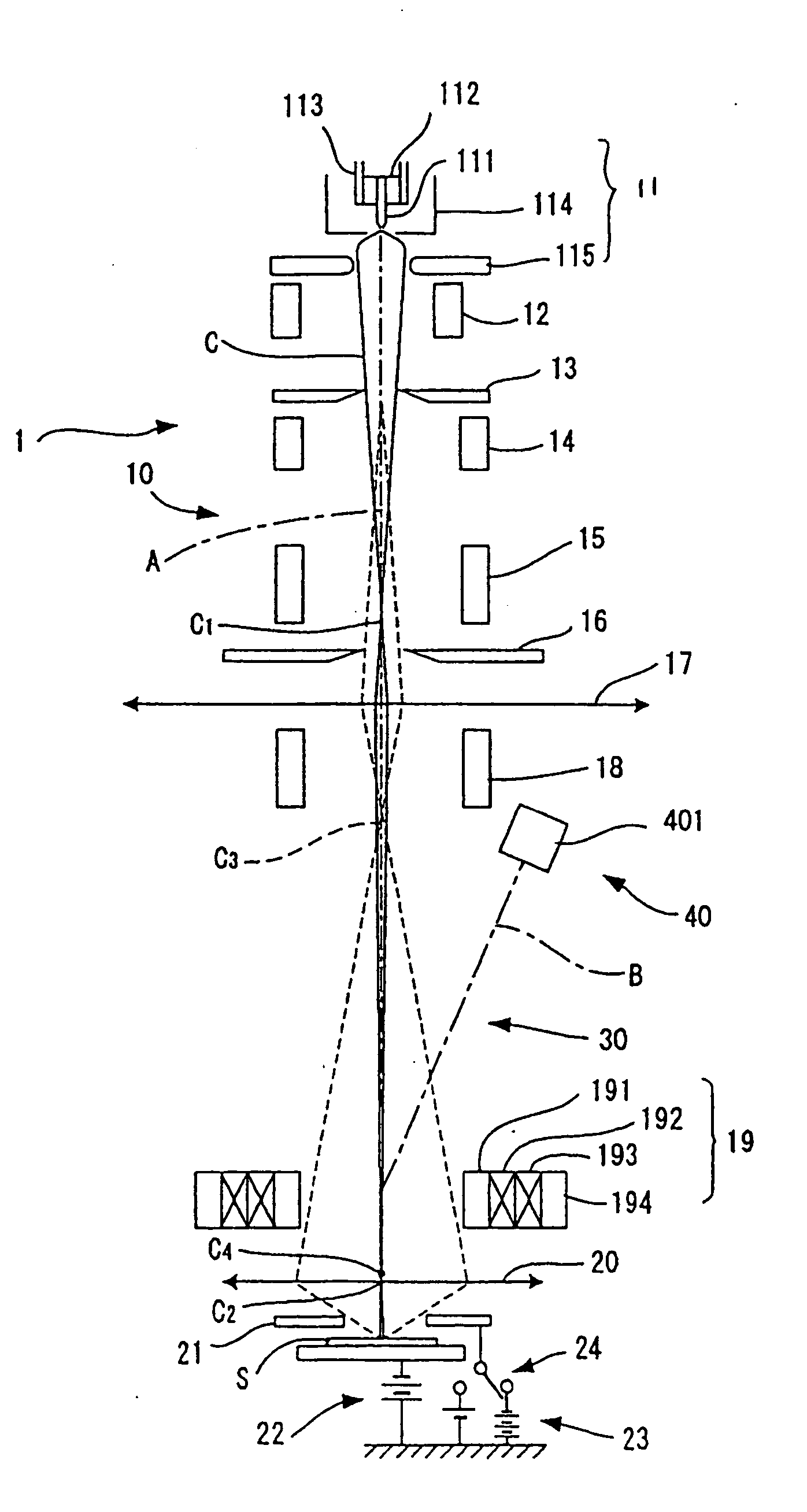
Figure 1 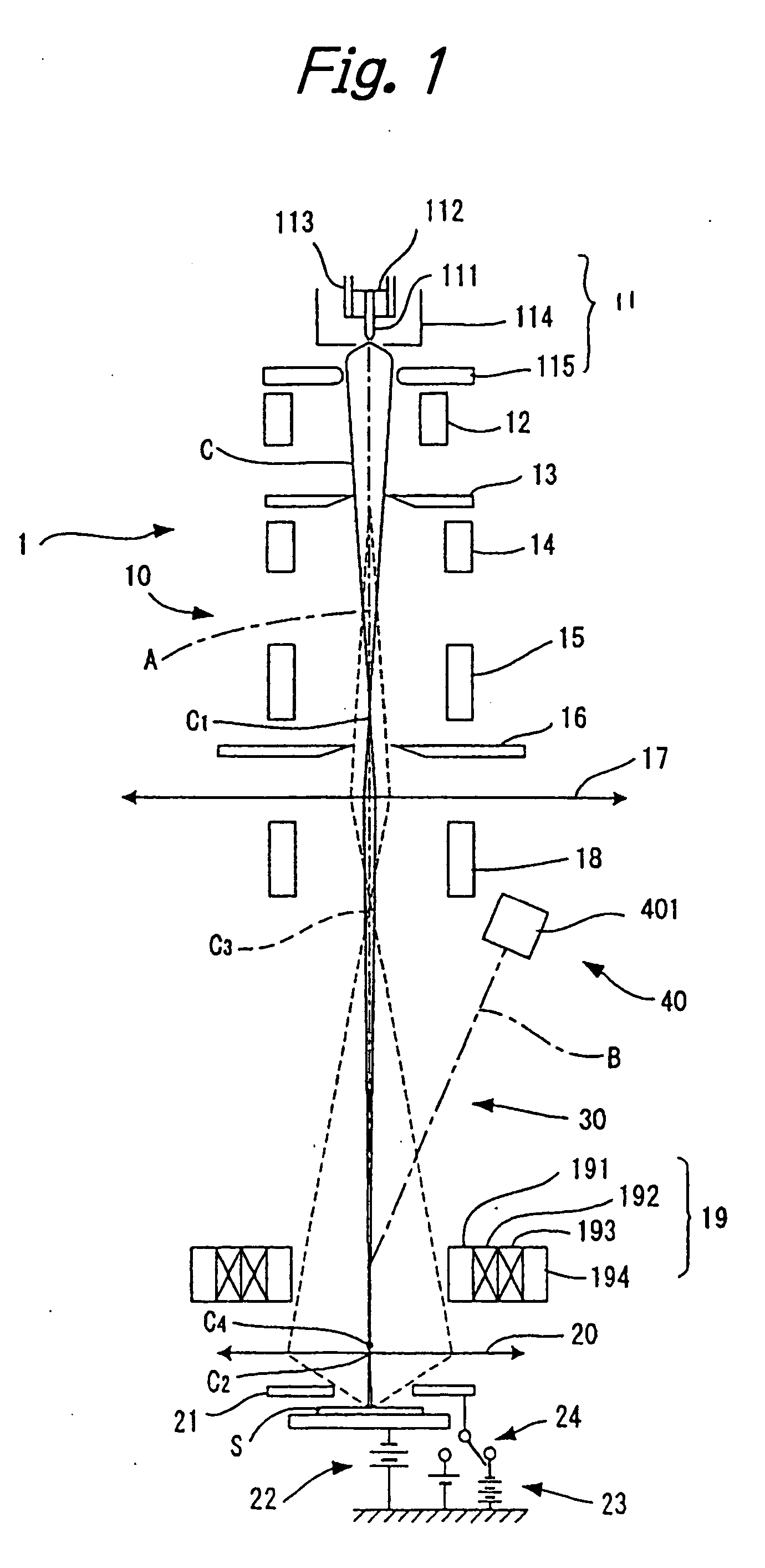
Figure 2 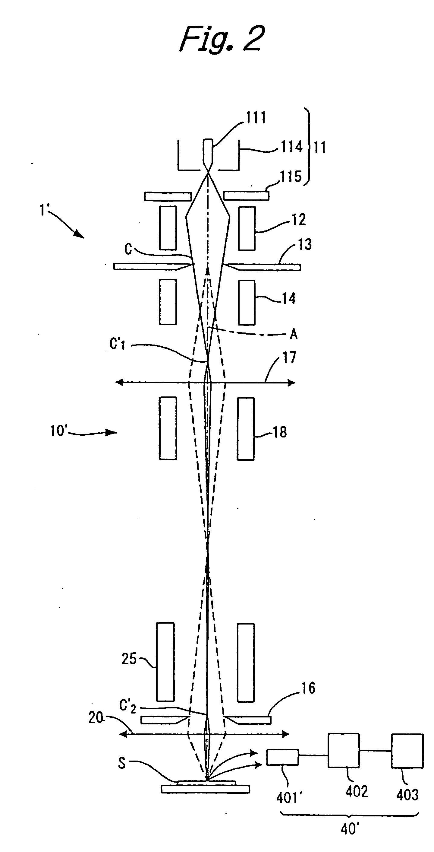
Figure 3
Abstract
Description
BACKGROUND OF THE INVENTION
[0001] The present invention relates to an electron beam system, a defect inspection apparatus for a device, which employs the same electron beam system, and a manufacturing method of a device using the same defect inspection apparatus, and more specifically, relates to an electron beam system which can evaluate a sample (a semiconductor wafer) having a device pattern with a minimum line width equal to or less than 0.1 μm with both a high throughput and high reliability, a defect inspection apparatus for a device, which employs the same electron beam system, and a manufacturing method of a device which can improve a yield thereof by evaluating a wafer after it has been processed using the same defect inspection apparatus.
[0002] The present invention also relates to an electron beam system and a defect inspection method for evaluating a device, such as a wafer or a mask, having a pattern with a minimum line width in a range of 0.1 micron, and also to a me...
Examples
first embodiment
[0051] In the first embodiment, the electron gun 11 is implemented as a LaB6 electron gun of the thermionic emission type, which comprises a LaB6 cathode 111, a graphite heater 112, a support fittings 113, a Wehnelt electrode 114 and an anode 115. By adjusting a bias of the Wehnelt electrode 114 of the electron gun 11 to be deeper to some extent, the electron gun 11 can be controlled within a space charge limited condition. The shaping aperture 13 is square in shape and disposed in a location in the electron gun side with respect to the NA aperture 16. Further, both of the two-stage lenses (i.e., the condenser lens 17 and the objective lens 20) are disposed in front locations of the shaping aperture 13 and the NA aperture 16 (i.e., in the sample side which is in a forward side with respect to the direction along which the electron beam advances).
[0052] The secondary optical system 30 is serving as an optical system for introducing secondary electrons emanated from the sample S into ...
second embodiment
[0062] An operation of the electron beam system having the configuration designated above will now be described. An electron beam “C” emitted from the electron gun 11 passes through the shaping aperture 13 to form a crossover image “C1′” in a predetermined location between the shaping aperture 13 and the condenser lens 17, and then the beam is dispersed from the crossover image C1′ at a spreading angle that is not too great. The dispersed electron beam is converged by the condenser lens 17 to form a crossover image “C2′” in the NA aperture 16. After forming the crossover image C2′, the electron beam proceeds toward the sample S and is directed to the sample S by the objective lens 20. An image of the shaping aperture 13 is demagnified by the condenser lens 17 and the objective lens 20 into the image on the sample S. In order to scan the sample, the beam is deflected in a two-stage manner by using the electrostatic deflector 18 and the electrostatic deflector 25 for scanning.
[0063] ...
third embodiment
[0065] Some further embodiments of the present invention will now be described below with reference to FIG. 3 to FIG. 6. FIG. 3 shows one example of configuration of an electron optical system in an electron beam system according to the present invention. In FIG. 3, an electron gun 11 comprises a cathode 201 made of LaB6 single crystal, a Wehnelt 202 and an anode 203, which are operated within a space charge limited condition. A primary electron beam emitted from the electron gun 11 is converged by a first condenser lens 204 to form a crossover image in a second aperture plate 205. A first aperture plate 206 has a square opening and thereby enables a high beam current (an intensified primary electron beam) to be obtained. It is to be noted that if a slightly deteriorated resolution in any specific direction is permissible, then a rectangular opening, instead of the square opening, may be used. The first aperture plate 206 having a shaping aperture is disposed downstream to the first...