
Direct demodulation method and apparatus
a demodulation method and signal technology, applied in the field of demodulation of signals, can solve the problems of circuits that are both relatively expensive and consume significant power, circuits that are limited in the data rate that they can handle, and the cost ofpagers, size and power consumption
Patent Information
- Authority / Receiving Office
- US · United States
- Current Assignee / Owner
- Publication Date
- 2000-01-04
- Estimated Expiration
- Not applicable · inactive patent
Smart Images
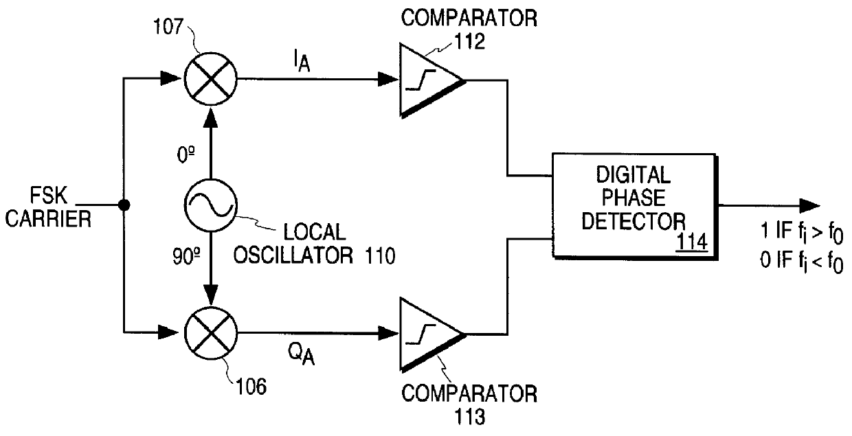
Figure 1 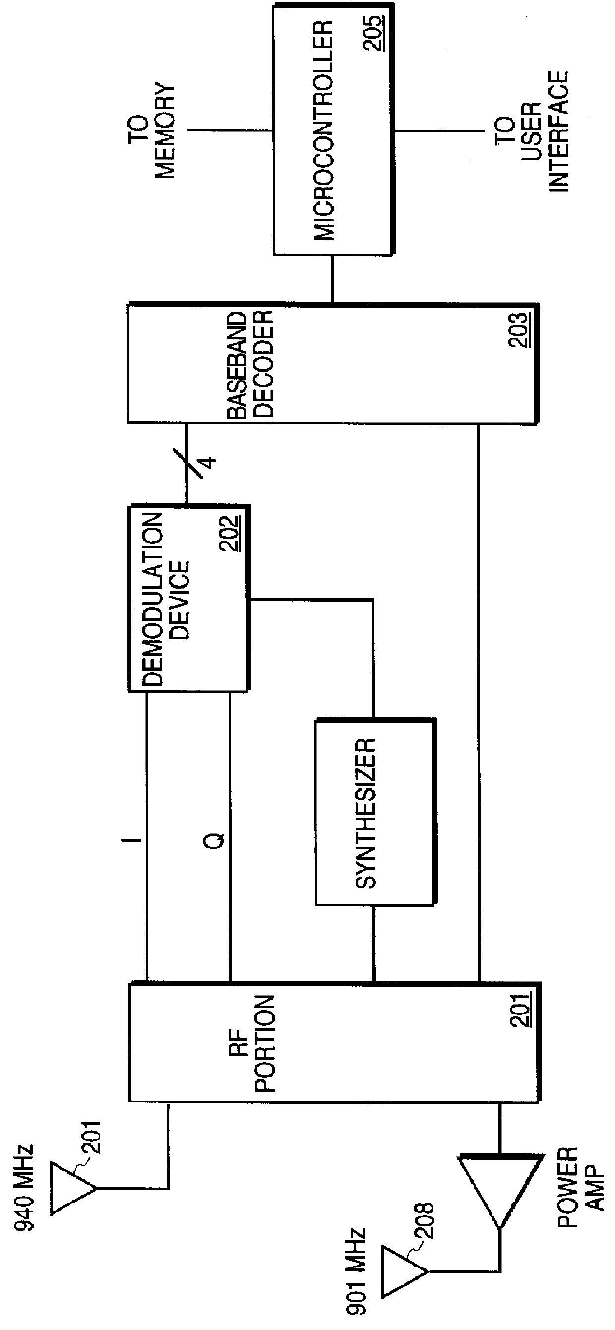
Figure 2 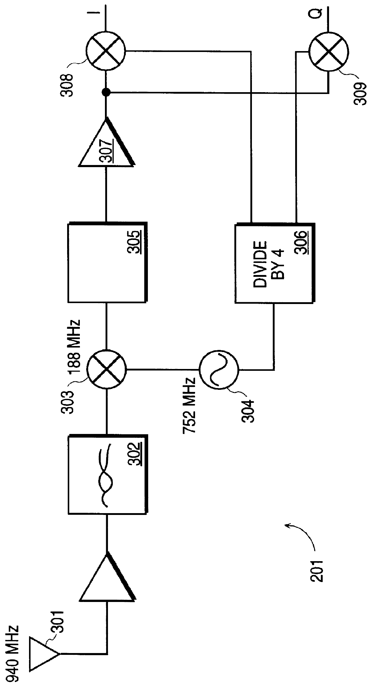
Figure 3
Abstract
Description
1. Field of the InventionThe present invention relates to the field of demodulation of signals. In its preferred embodiment, the present invention has application in communication devices such as pagers.2. Description of the Related ArtPagers have gained popularity in recent years. Several key issues in the design of pagers are cost, size and power consumption. Very briefly, a pager receives radio frequency (RF) signals, converts them to digital signals, and displays resulting messages or takes other action (such as control of functions of the pager) based on the received signals. The conversion process from RF signals to digital signals requires several steps including converting the RF signal to a baseband and demodulation of the signal to digital representations of the signal. Of course, the conversion approach will vary dependent on the selection of a particular digital modulation technique.Typical prior art approaches to conversion of the RF signal employ discrete analog circui...
Examples
Embodiment Construction
of the Direct Demodulation Circuit of the Present Invention
A. RF Receiver 201 (FIG. 3)
Turning now to FIG. 3, an RF receiver as may be utilized by the present invention is illustrated. The antenna 301 provides a 940 MHz FSK modulated signal to image reject filter 302. The image reject filter 302 removes the image frequencies and has its output coupled to mixer 303. Oscillator 304 provides a 752 MHz signal as a second input to mixer 303. Mixer 303 provides as an output a signal converted as IF frequency which is then fed as an input to filter 305. The filtered baseband signal is fed to amplifier 307. Amplifier 307 provides as an output an amplified signal which is then provided as inputs to I / Q mixers 308 and 309.
The 752 MHz signal from the oscillator is divided by 4 by divider 306. Divider 306 provides two output at 188 MHz differentiated by a 90.degree. phase shift which are used as second inputs to mixers 308 and 309. Mixers 308 and 309 provide I and Q output signals, respectively....