
Forming solder balls on substrates
a technology of substrates and solder balls, which is applied in the direction of soldering apparatus, non-printed masks,auxillary welding devices, etc., can solve the problems of high cost of metal mask replacement, inconvenient and inability to meet the needs of fine pitch ball bumping
Patent Information
- Authority / Receiving Office
- US · United States
- Current Assignee / Owner
- Publication Date
- 2006-03-07
- Estimated Expiration
- Not applicable · inactive patent
Smart Images
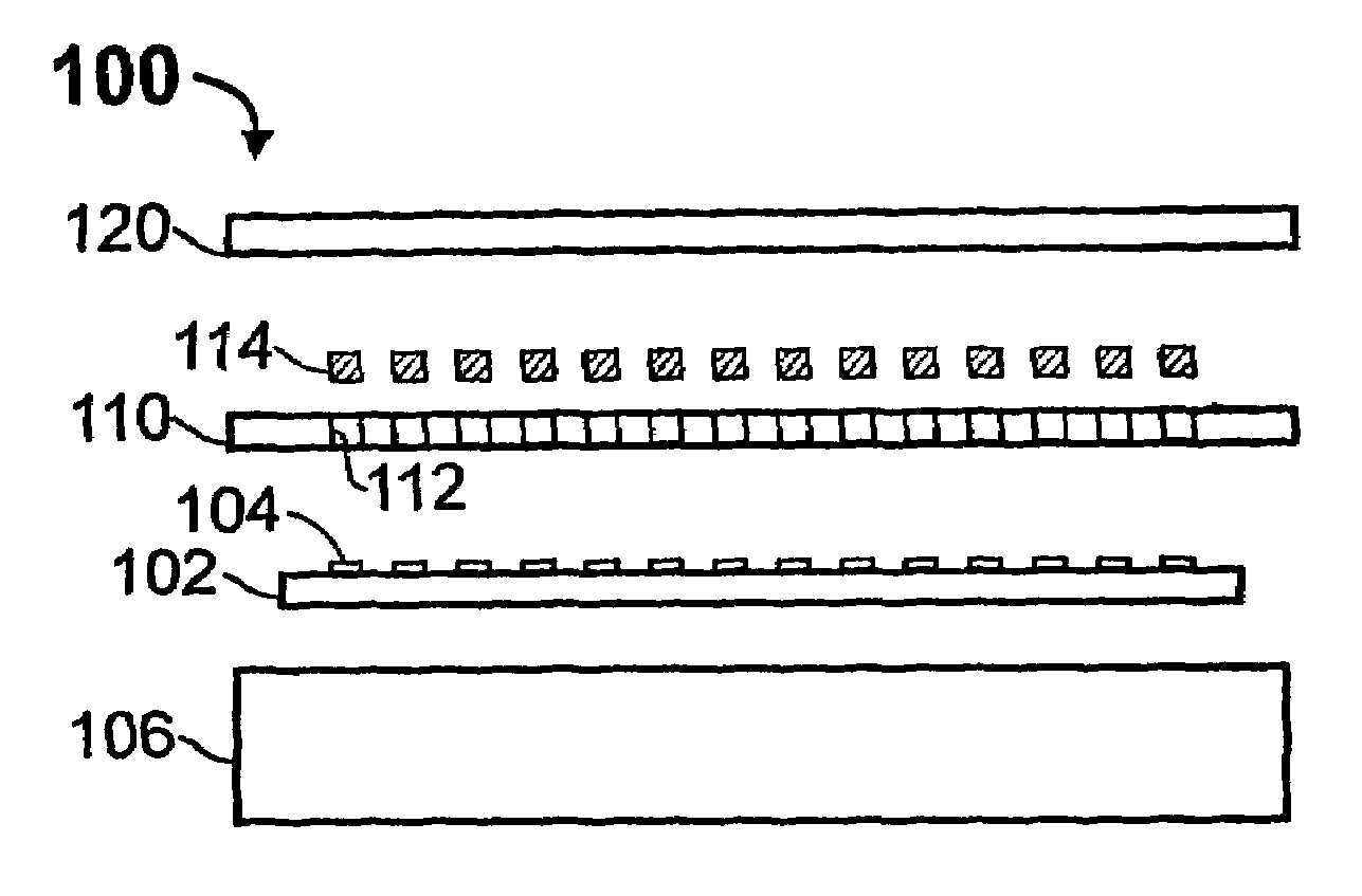
Figure 1 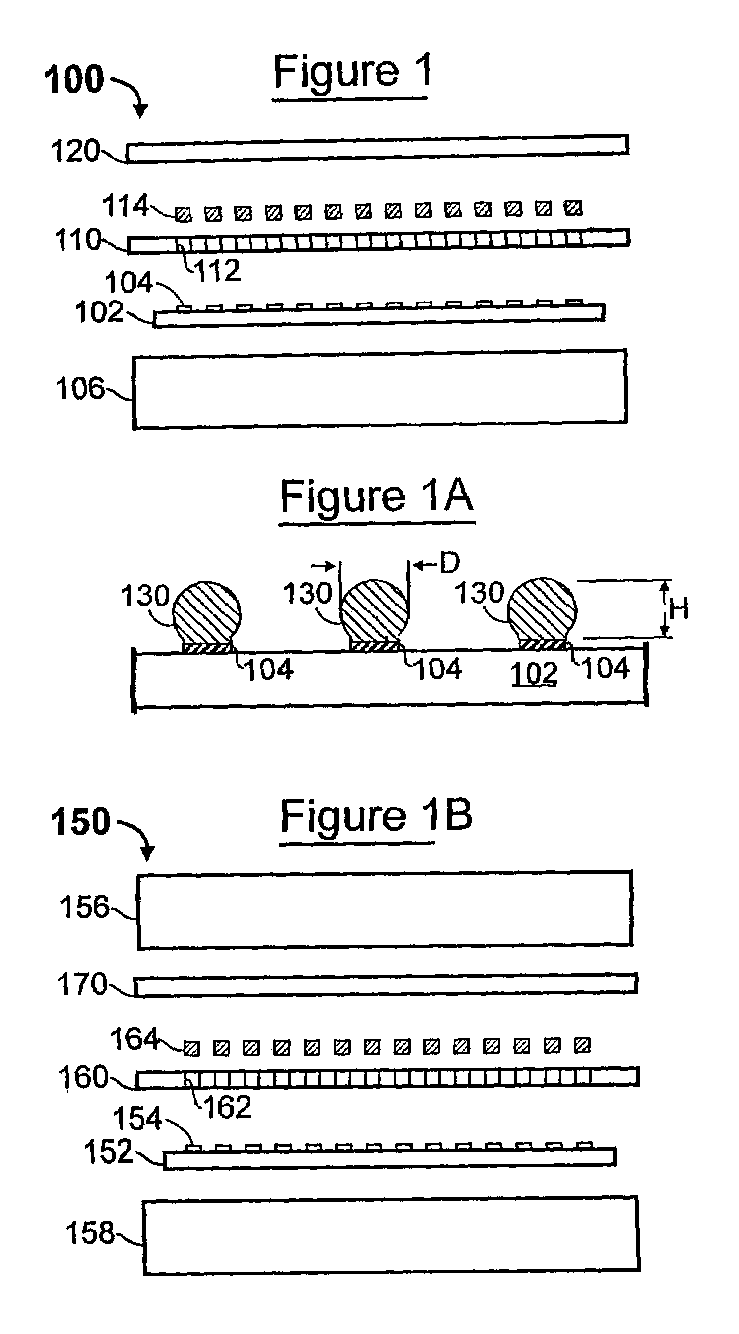
Figure 2 
Figure 3
Abstract
Description
CROSS-REFERENCES TO RELATED APPLICATIONS
[0001] This application is a continuation-in-part of:
[0002] Ser. No. 09 / 962,007 filed Sep. 24, 2001 (issuing as U.S. Pat. No. 6,609,652, Aug. 26, 2003) which is a continuation-in-part of:
[0003] U.S. Ser. No. 09 / 273,517 filed Mar. 22, 1999 (U.S. Pat. No. 6,293,456, Sep. 25, 2001), which is a continuation-in-part of each of:
[0004] U.S. Ser. No. 08 / 863,800 filed 27 May 1997 (U.S. Pat. No. 5,988,487, Nov. 23, 1999);
[0005] U.S. Ser. No. 60 / 079,006 filed 23 Mar. 1998;
[0006] U.S. Ser. No. 60 / 079,221 filed 24 Mar. 1998; and
[0007] U.S. Ser. No. 60 / 092,055 filed 08 Jul. 1998,all of which are incorporated in their entirety by reference herein.
[0008] This application is also a continuation-in-part of:
[0009] U.S. Ser. No. 10 / 630,310 filed Jul. 30, 2003 as a continuation-in-part of the aforementioned Ser. No. 09 / 962,007.TECHNICAL FIELD OF THE INVENTION
[0010] The invention relates to methods of forming solder balls on substrates which are electronic components such as...
Examples
Embodiment Construction
[0110]FIG. 1 illustrates a technique 100 for forming solder balls on a surface of a substrate 102, such as is set forth in “parent” U.S. patent application Ser. No. 08 / 863,800 (U.S. Pat. No. 5,988,487, Nov. 23, 1999), incorporated in its entirety by reference herein.
[0111]The substrate 102 has number of pads 104 on its top (as viewed) surface. The pads 104 are typically arranged in an array, having a pitch (center-to-center spacing from one another). The substrate 102 is disposed atop a heater stage 106.
[0112]A mask (stencil) 110 is provided. The mask 110 is a thin planar sheet of relatively stiff material, such as molybdenum, having a plurality of openings (cells) 112, each corresponding to a pad 104 whereupon it is desired to form a solder ball on the substrate 102.
[0113]The mask 110 is placed on the top (as viewed) surface of the substrate 102 with the cells 112 aligned over the pads 104. The cells 112 in the mask 110 are filled with solder material 114. This is done in any suita...