
Method for forming radio frequency antenna
a radio frequency antenna and antenna technology, applied in the field of radio frequency antennas, can solve the problems of unreliability and prone to failure, and achieve the effects of reducing the resistance between the electrode and the other locations on the conductive ink layer, and reducing the risk of failur
Patent Information
- Authority / Receiving Office
- US · United States
- Patent Type
- Patents(United States)
- Current Assignee / Owner
- Publication Date
- 2007-11-20
- Estimated Expiration
- Not applicable · inactive patent
Smart Images
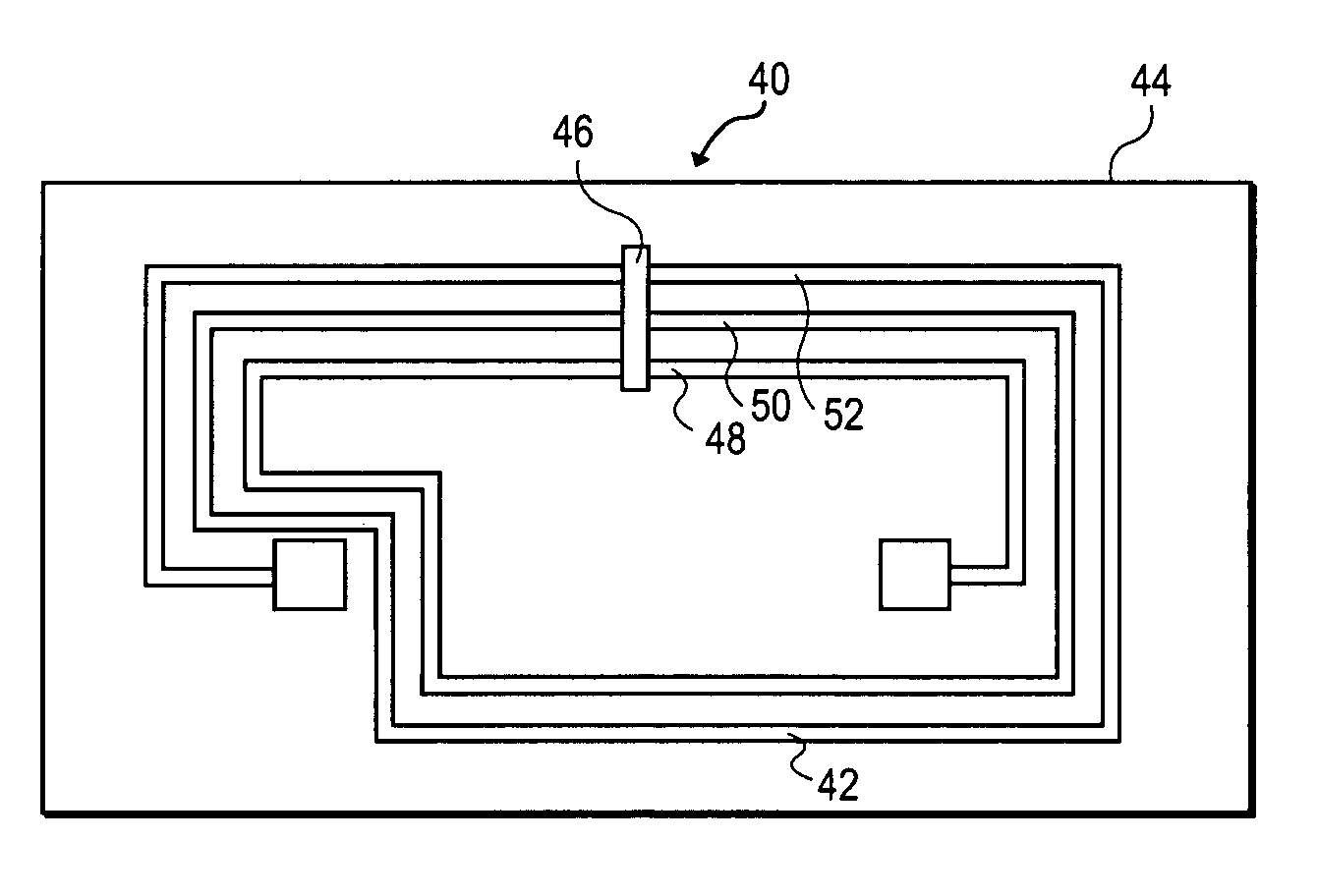
Figure 1 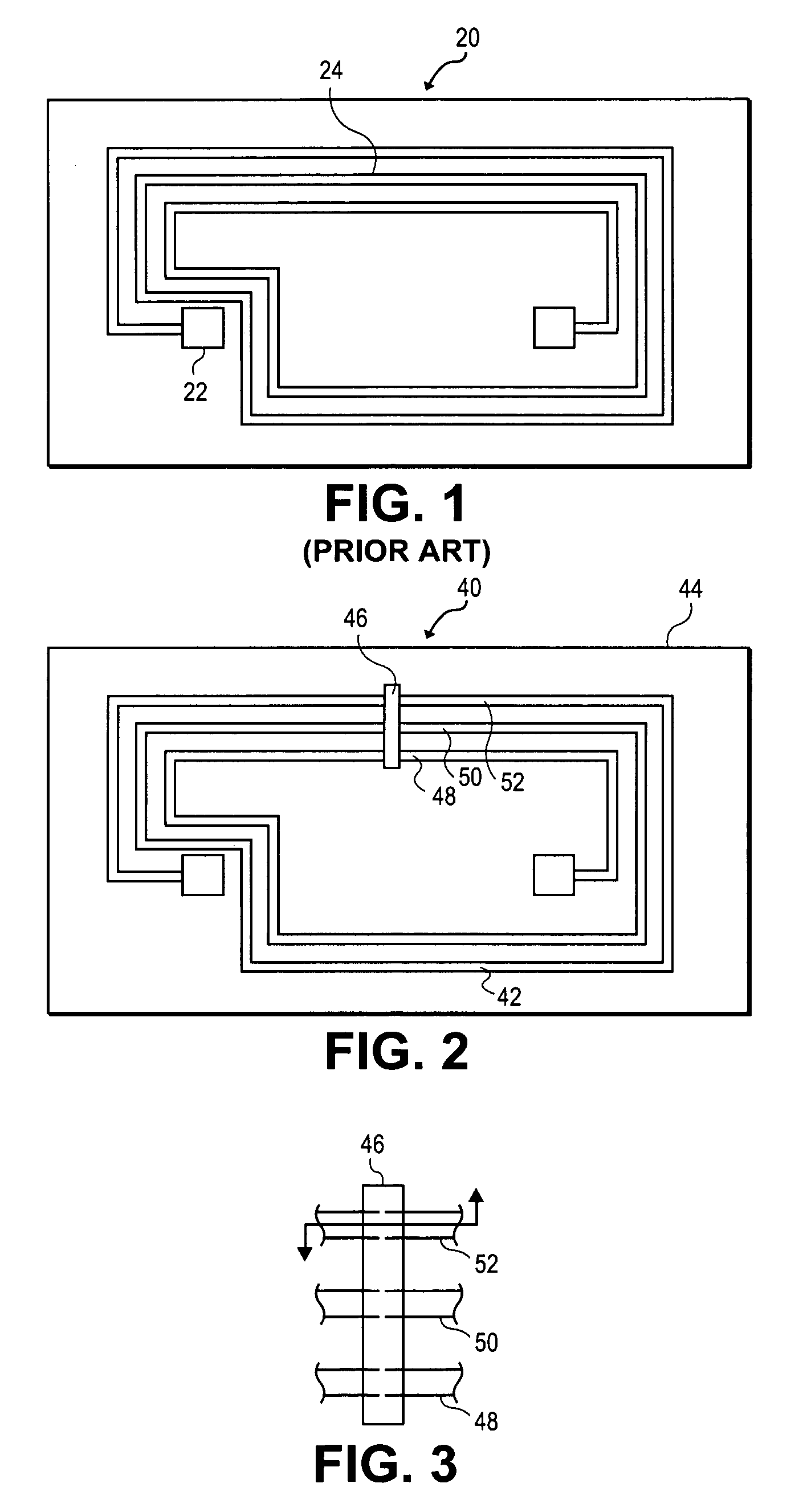
Figure 2 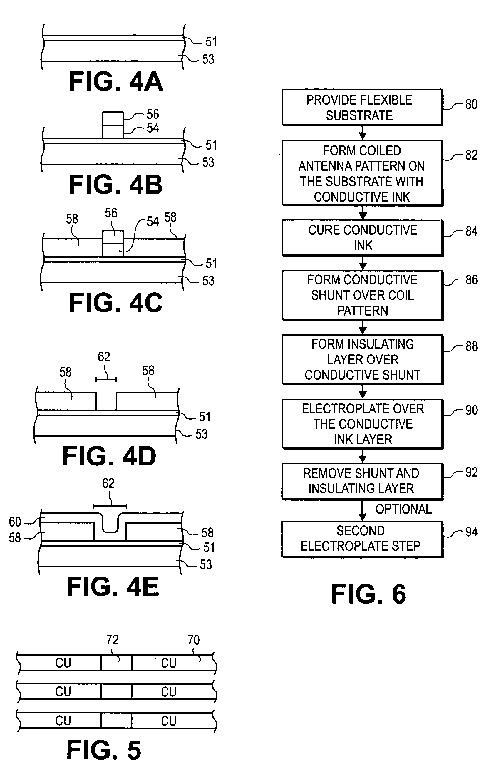
Figure 3
Abstract
Description
CLAIM OF PRIORITY
[0001] This application is a continuation in part of U.S. patent application Ser. No. 10 / 925,229 filed Aug. 24, 2004, now U.S. Pat. No. 7,268,740 which is a continuation in part of U.S. patent application Ser. No. 10 / 238,598 filed Sep. 11, 2002, now U.S. Pat. No. 6,933,892 which is a continuation of U.S. patent application Ser. No. 09 / 524,505 filed Mar. 13, 2000 now U.S. Pat. No. 6,476,775.BACKGROUND OF THE INVENTION
[0002] The present invention relates to methods of manufacture of flexible circuits used in construction of radio frequency (RF) antennae.
[0003] Radio frequency antennae are typically made in a conductive coil pattern. The conductive coil pattern allows the antenna to receive and radiate energies in the radio frequency range. Typically, the antenna is optimized to transmit and receive energy in a relatively narrow portion of the radio frequency range.
[0004] Radio frequency antennae are used in a number of different areas including inventory control. Often th...
Examples
Embodiment Construction
[0024]FIG. 2 is a top view of a radio frequency antenna 40 being constructed by the method of one embodiment of the present invention. The radio frequency antenna 40 includes a conductive ink pattern 42 formed in a coil on the substrate 44. An electrical-short layer 46 is formed over top of the conductive ink coil pattern, and preferably a nonconductive plating resist is formed over the short. The electrical-short layer 46 ensures that points 48, 50 and 52 on the conductive ink pattern 42 will have relatively similar voltages during the electroplating process. This means all locations on the conductive ink pattern 42 will be electroplated evenly. Thus the apparatus of the present invention allows for a conductive electroplate layer of sufficient thickness on all points of the radio frequency antenna.
[0025]The use of the electrical-short layer 46 allows for the use of a thinner and / or narrower conductive ink layer 42. The resistance of the conductive ink layer during the electroplate...