
Field effect transistor
a field effect transistor and transistor technology, applied in the field of field effect transistors, can solve the problems of scaling having its limits, and achieve the effect of selectively increasing the effective channel length (leff) and the transistor siz
Patent Information
- Authority / Receiving Office
- US · United States
- Patent Type
- Patents(United States)
- Current Assignee / Owner
- Publication Date
- 2009-03-31
- Estimated Expiration
- Not applicable · inactive patent
Smart Images
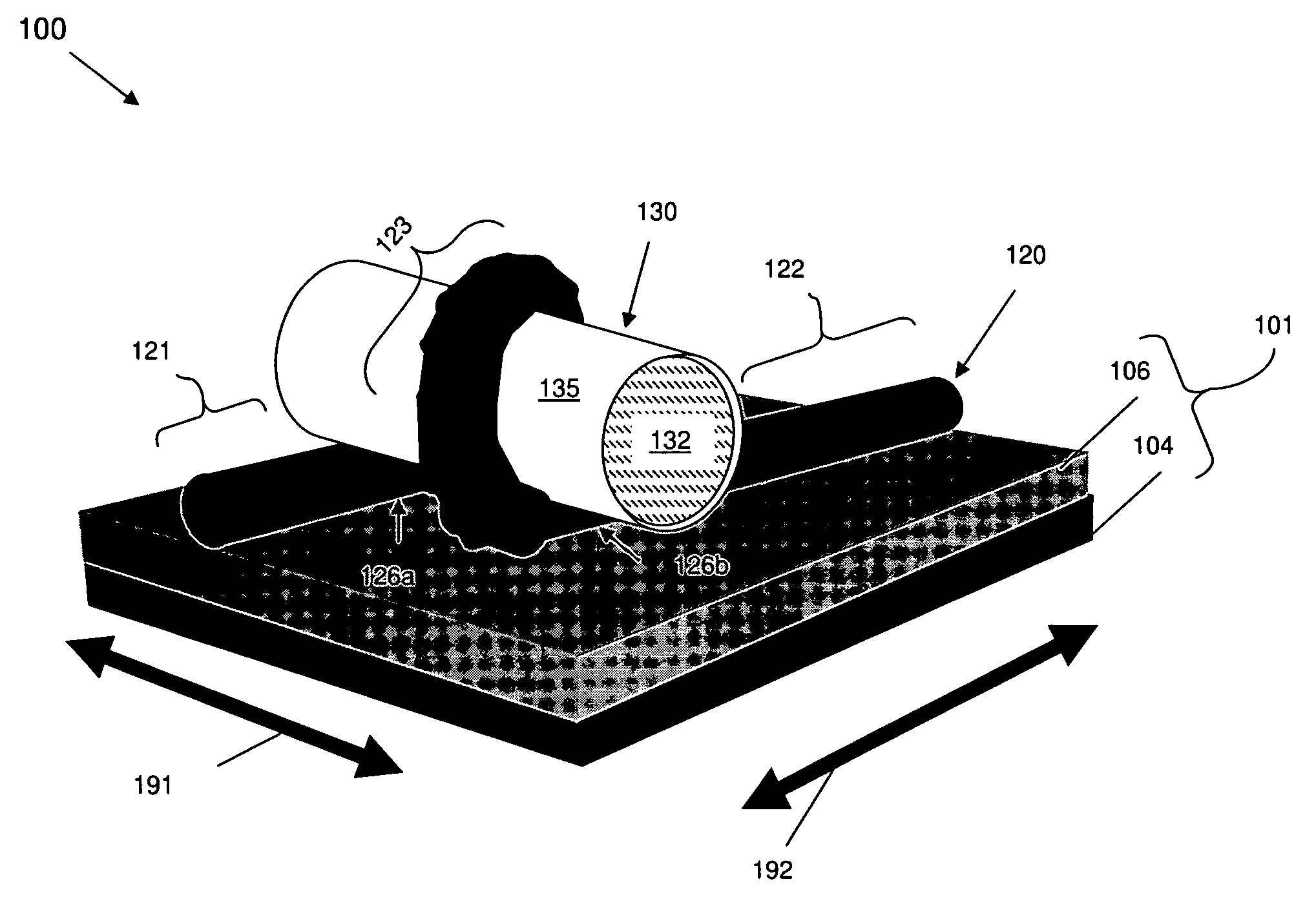
Figure 1 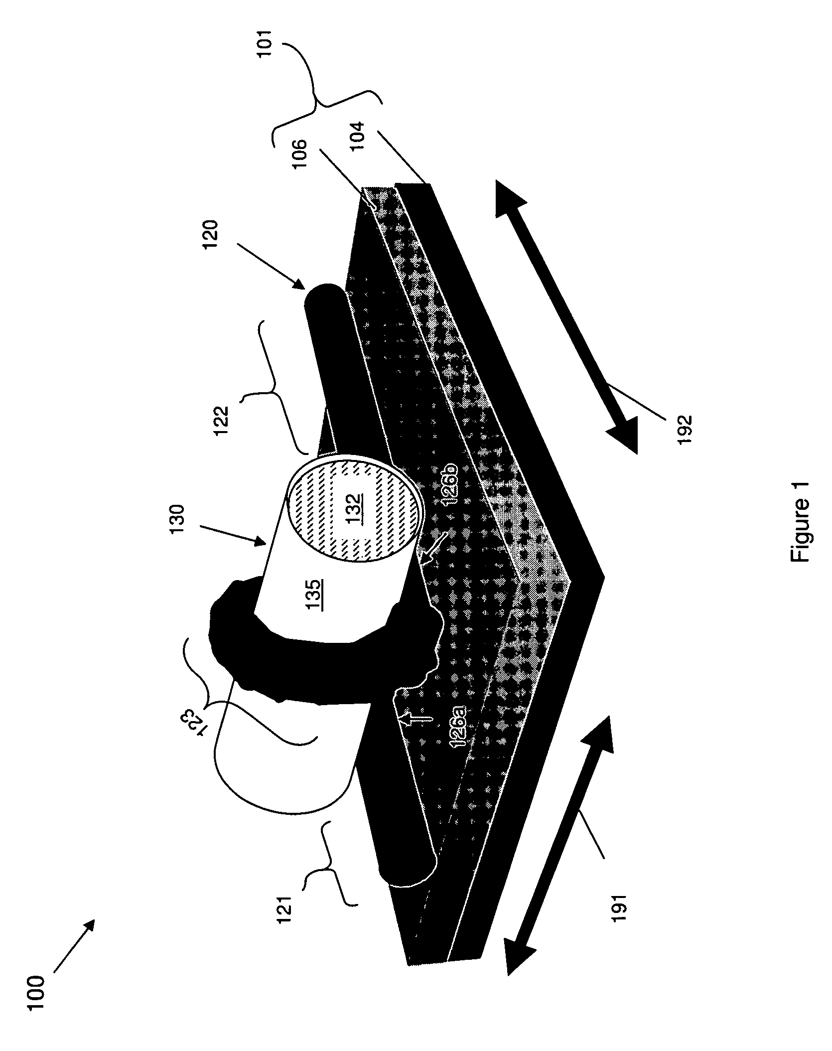
Figure 2 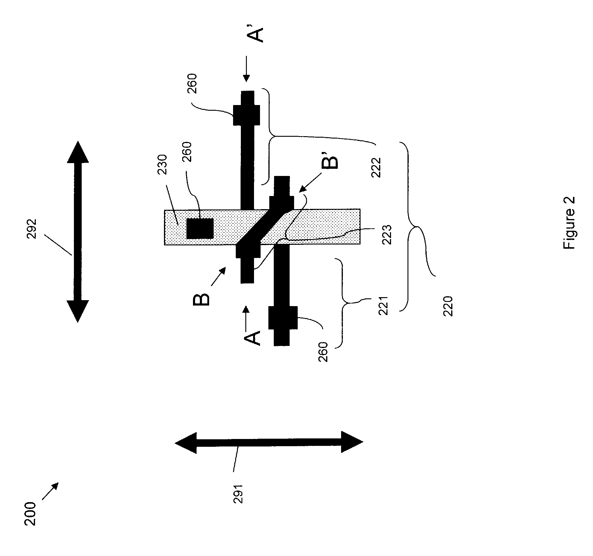
Figure 3
Abstract
Description
BACKGROUND
[0001] 1. Field of the Invention
[0002] The embodiments of the invention generally relate to field effect transistors and, more particularly, to a field effect transistor having an increased effective channel length (Leff).
[0003] 2. Description of the Related Art
[0004] Over the past few decades numerous performance and economic advantages have been seen with semiconductor technology scaling. For example, transistor size scaling has lead to decreased channel lengths and a corresponding increase in switching speeds (i.e., shorter channel lengths correspond to faster switching speeds). However, recently it has been determined that such scaling has its limits because short channel lengths can lead to undesirable “short-channel effects” including, but not limited, variability in threshold voltage and excessive drain leakage currents. Therefore, there is a need in the art for an improved transistor that allows for transistor size scaling without decreasing the effective channel lengt...
Examples
embodiment 100
[0074]More particularly, referring to FIG. 8, a transistor embodiment 100 of FIG. 1 with a carbon nanotube semiconductor body 120 can be formed, for example, by providing a multi-layer substrate (802). For example, a substrate 101a can be provided that comprises an isolation layer 106a (e.g., an oxide layer or other dielectric layer) on a conductor layer 104a (e.g., a doped semiconductor layer, such as a doped silicon or polysilicon layer, or a metal layer) (see FIG. 9a). Alternatively, a substrate 101b can be provided that comprises isolation layer 106b (e.g., a quartz layer or an oxide layer) on a semiconductor layer 104b (e.g., on a silicon layer) (see FIG. 9b). Then, a carbon nanotube 120 can be formed (e.g., deposited) on the substrate 101a, 101b (804, see FIGS. 9a and 9b).
[0075]This carbon nanotube 120 can be formed using conventional carbon nanotube processing techniques, for example, arc evaporation, or passing of carbon-containing gases over nanoparticles of Co, Fe, or Ni, ...
embodiment 200
[0079]Alternatively, referring to FIG. 21, the transistor embodiment 200 of FIGS. 2-4 with a polysilicon or silicon semiconductor body 220 can be formed, for example, by first providing a wafer comprising a multi-layer substrate 201 (2102, see FIG. 22). For example, the substrate 201 can comprise an isolation layer 206 (e.g., an oxide layer or other dielectric layer) on at least one additional layer 204. This additional layer 204 can comprise a conductor layer (e.g., a doped semiconductor layer, such as a doped silicon or polysilicon layer, or a metal layer) immediately below the isolation layer. Alternatively, this additional layer 204 can comprise semiconductor layer (e.g., on a silicon layer) below the isolation layer 106. Then, an undoped (i.e., intrinsic) semiconductor layer 208 (e.g., an undoped polysilicon layer or an undoped silicon layer) is formed (e.g., deposited) onto the isolation layer 206 (2104).
[0080]After the semiconductor layer 208 is formed at process 2104, shallo...