
Semiconductor memory device and method of operating the same
a memory device and semiconductor technology, applied in the field of semiconductor memory devices, can solve the problems of difficult to raise the breakdown voltage of a pass transistor
Patent Information
- Authority / Receiving Office
- US · United States
- Patent Type
- Patents(United States)
- Current Assignee / Owner
- Publication Date
- 2013-08-27
Smart Images
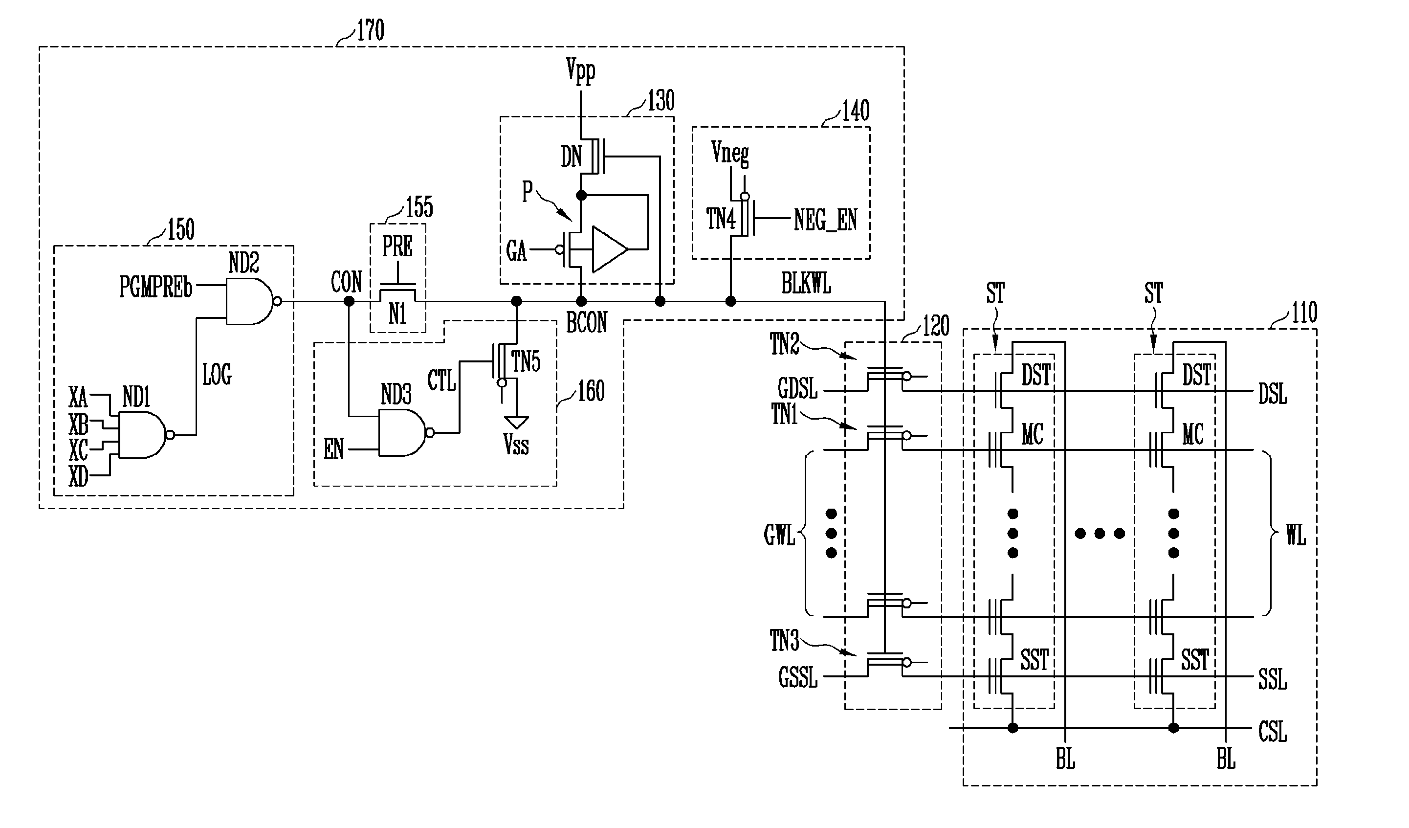
Figure 1 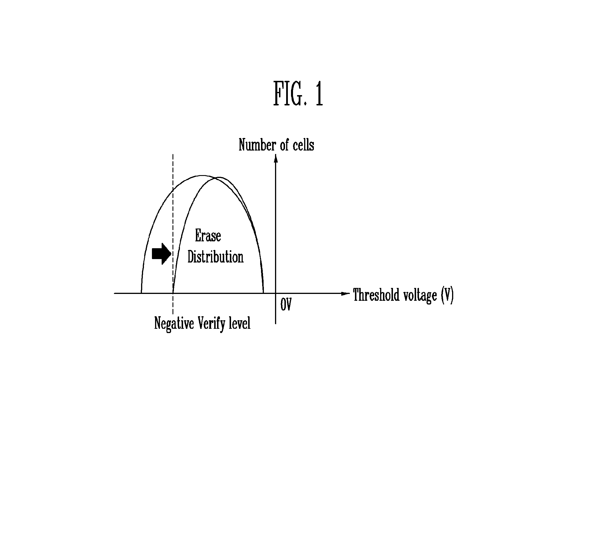
Figure 2 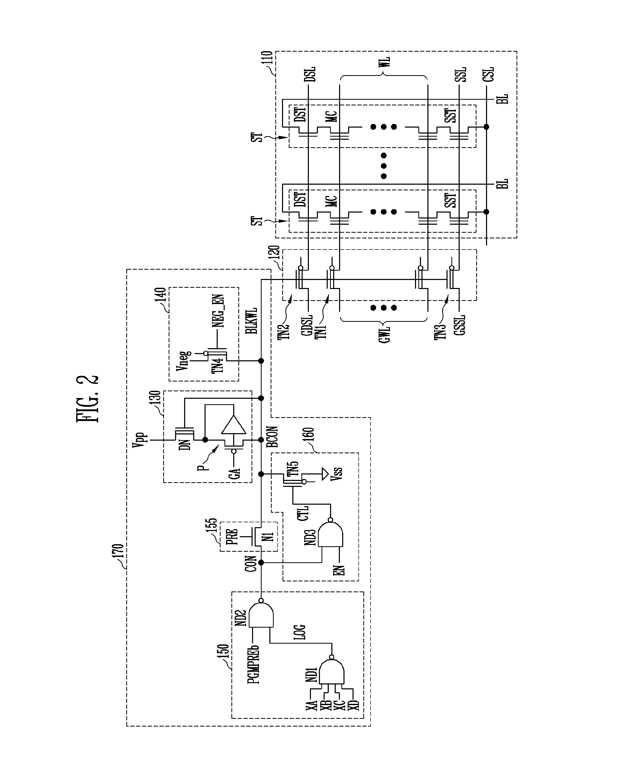
Figure 3
Abstract
Description
CROSS-REFERENCE TO RELATED APPLICATION
[0001] Priority is claimed to Korean patent application number 10-2010-0085444 filed on Sep. 1, 2010, the entire disclosure of which is incorporated herein by reference in its entirety.BACKGROUND
[0002] Exemplary embodiments relate to a semiconductor memory device and more particularly to securing sufficient margin between threshold voltage distributions in a semiconductor memory device.
[0003] Data storage capacity of a memory device can be increased by configuring each memory cell to store more than one bit. There then could be four or more distributions of memory cell threshold voltages. There may be three or more distributions of threshold voltages of the memory cells in a program state as well as the distribution of threshold voltages of memory cells in an erase state. These distributions must be secured with a sufficient margin between them in order to determine without error as to which distribution of what state belongs the certain threshold ...
Examples
Embodiment Construction
[0028]Hereinafter, some exemplary embodiments of the present disclosure will be described in detail with reference to the accompanying drawings. The figures are provided to allow those having ordinary skill in the art to understand the scope of the embodiments of the disclosure.
[0029]FIG. 1 illustrates one example of the threshold voltage distribution of memory cells in an erase state.
[0030]Referring to FIG. 1, a negative threshold voltage is associated with each of the memory cells in an erase state. In a program operation, the threshold voltage of a program state, which is higher than the threshold voltage of an erase state, is associated with each of the memory cells. When the erase state threshold voltage distribution of the memory cells is not made sufficiently narrow, there may be present a less-than-sufficient margin between the threshold voltage distributions of a program state. In order to secure the margin between the threshold voltage distributions of the memory cells in ...