
Laser devices using a semipolar plane
a laser device and semi-polar plane technology, applied in the field of optical devices, can solve the problems of 0.1% efficiency of wall plugs, 80% power consumption, routine failure, etc., and achieve the effect of reducing the degradation of quantum wells or light emitting regions, low resistance p-cladding, and good device performan
Patent Information
- Authority / Receiving Office
- US · United States
- Patent Type
- Patents(United States)
- Current Assignee / Owner
- Publication Date
- 2015-10-20
Smart Images
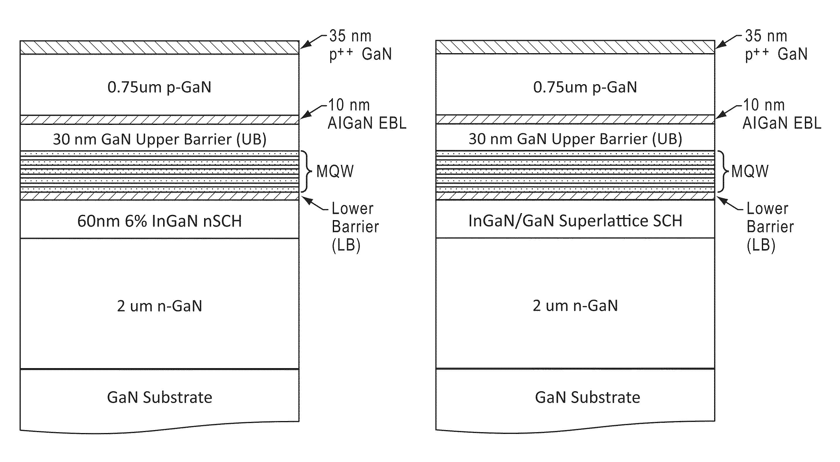
Figure 1 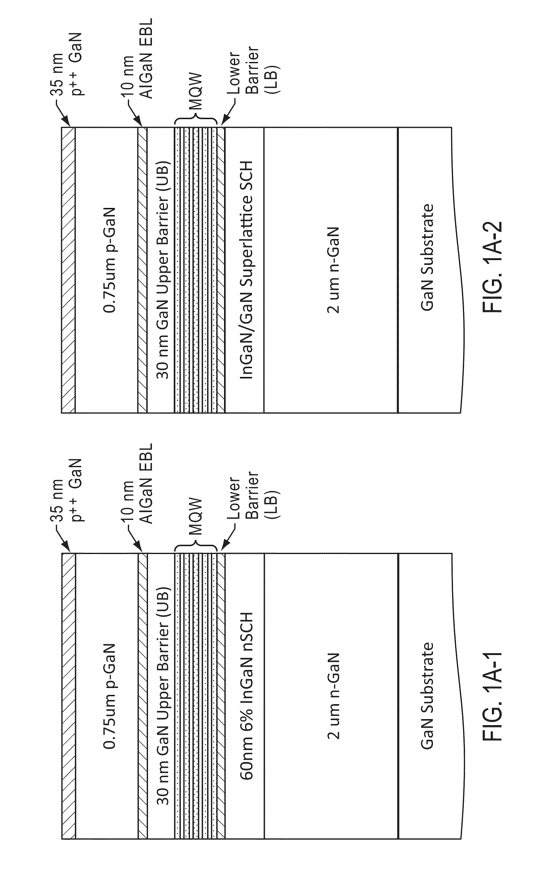
Figure 2 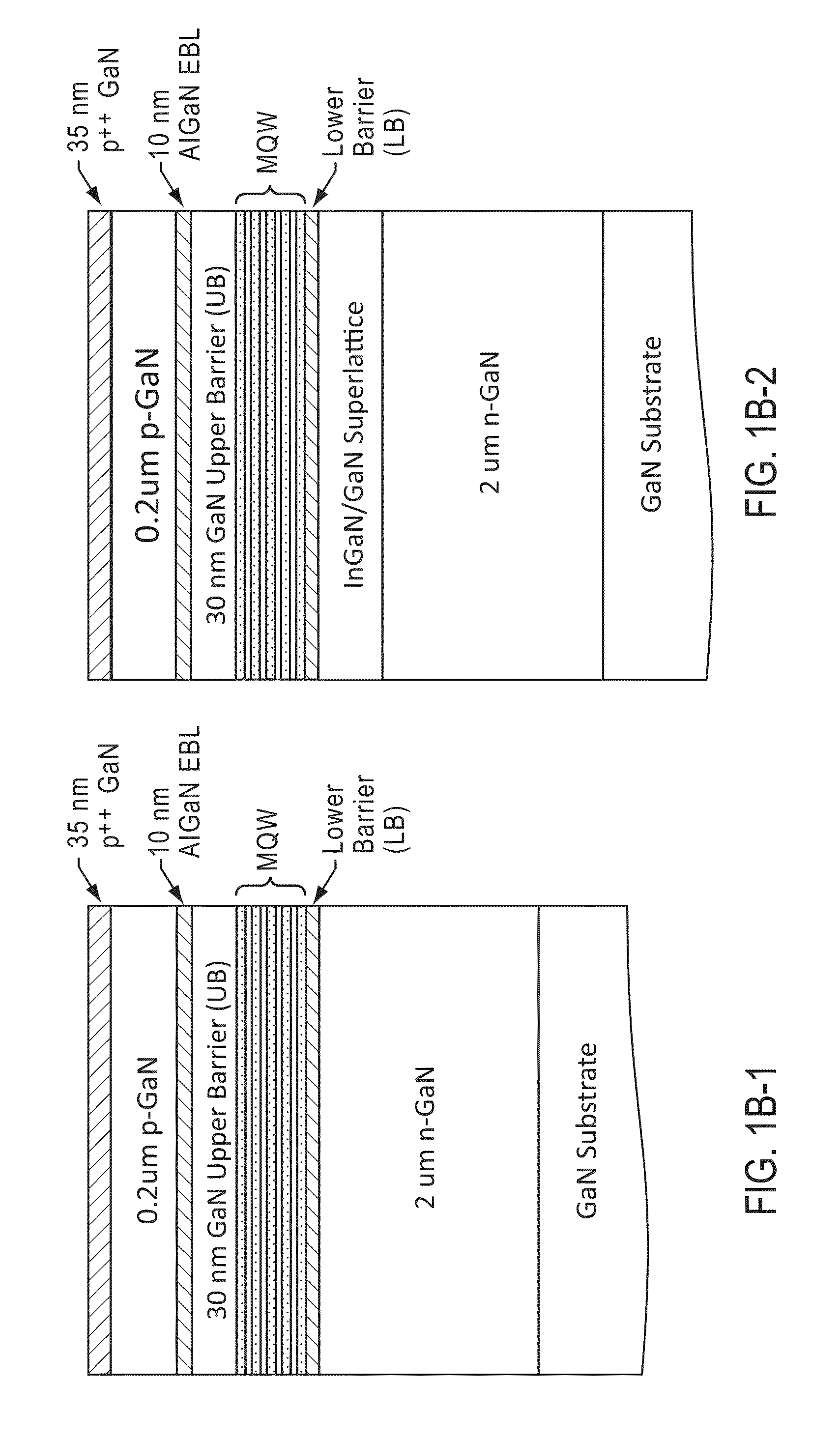
Figure 3
Abstract
Description
[0001] This application is a continuation of U.S. application Ser. No. 13 / 651,291, filed Oct. 12, 2012, which claims the benefit of U.S. Provisional Application No. 61 / 546,792 filed on Oct. 13, 2011, both of which are incorporated by reference herein in their entirety.BACKGROUND
[0002] The present invention is directed to optical devices and related methods. In particular, the invention provides a method and device for emitting electromagnetic radiation using nonpolar or semipolar gallium containing substrates such as GaN, AlN, InN, InGaN, AlGaN, and AlInGaN, and others. More particularly, the present invention provides a method and device using a gallium and nitrogen containing substrate configured on the {20-21} family of planes or an off-cut of the {20-21} family of planes toward the plus or minus c-plane and / or toward the a-plane according to one or more embodiments, but there can be other configurations. Such family of planes include, but are not limited to, (30-3-2), (20-2-1), (3...
Examples
Embodiment Construction
[0053]FIGS. 1A-1, 1A-2, 1B-1, and 1B-2 are diagrams of optical devices including growth regions according to an embodiment of the present invention. As shown, the laser diode is an epitaxial structure configured on a gallium and nitrogen containing substrate within a family of planes, e.g., (30-3-2), (20-2-1), (30-3-1), (30-32), (20-21), (30-31) or any orientation within + / −10 degrees toward c-plane and / or a-plane from these orientations. In a specific embodiment referring to FIG. 1A-1, the gallium nitride substrate includes an n-type gallium and nitride epitaxial region, an overlying InGaN nSCH region, a lower barrier region, a plurality of quantum well regions, an upper barrier region, an electron blocking region, a p-type gallium and nitrogen containing region, and an overlying p++ GaN contact region. Referring now to FIG. 1A-2, the gallium nitride substrate includes an n-type gallium and nitride epitaxial region, an overlying InGaN / GaN superlattice SCH region, a lower barrier re...