

Advanced Reticle Inspection vs Conventional Techniques for Overlay Errors
MAY 20, 20269 MIN READ
Generate Your Research Report Instantly with AI Agent
PatSnap Eureka helps you evaluate technical feasibility & market potential.
Advanced Reticle Inspection Technology Background and Objectives
Advanced reticle inspection technology has emerged as a critical component in semiconductor manufacturing, addressing the increasingly stringent requirements for overlay accuracy in modern lithography processes. The evolution from conventional inspection methods to advanced techniques represents a fundamental shift in how the industry approaches defect detection and process control at the photomask level.
The semiconductor industry's relentless pursuit of smaller feature sizes and higher device densities has created unprecedented challenges in maintaining overlay accuracy. Traditional inspection methodologies, while effective for previous technology nodes, have reached their practical limitations when dealing with sub-10nm processes. These conventional techniques often rely on optical inspection systems with limited resolution capabilities and basic pattern recognition algorithms that struggle to detect subtle overlay errors that can significantly impact device performance.
Advanced reticle inspection technologies leverage cutting-edge optical systems, enhanced computational algorithms, and machine learning capabilities to achieve superior detection sensitivity and accuracy. These systems incorporate high-resolution imaging platforms, advanced illumination schemes, and sophisticated data processing techniques that enable the identification of overlay errors at unprecedented precision levels. The integration of artificial intelligence and deep learning algorithms has further enhanced the capability to distinguish between actual defects and false positives.
The primary objective of implementing advanced reticle inspection is to establish a robust quality control framework that ensures overlay specifications are met consistently across all production wafers. This involves developing inspection methodologies that can detect overlay errors with sub-nanometer precision while maintaining high throughput requirements essential for volume manufacturing. The technology aims to provide real-time feedback mechanisms that enable immediate process corrections, thereby minimizing yield loss and reducing manufacturing costs.
Furthermore, advanced reticle inspection seeks to establish predictive maintenance capabilities by identifying potential sources of overlay drift before they impact production yields. The integration of comprehensive data analytics platforms enables the correlation of inspection results with downstream process performance, facilitating continuous improvement in manufacturing efficiency and product quality standards.
The semiconductor industry's relentless pursuit of smaller feature sizes and higher device densities has created unprecedented challenges in maintaining overlay accuracy. Traditional inspection methodologies, while effective for previous technology nodes, have reached their practical limitations when dealing with sub-10nm processes. These conventional techniques often rely on optical inspection systems with limited resolution capabilities and basic pattern recognition algorithms that struggle to detect subtle overlay errors that can significantly impact device performance.
Advanced reticle inspection technologies leverage cutting-edge optical systems, enhanced computational algorithms, and machine learning capabilities to achieve superior detection sensitivity and accuracy. These systems incorporate high-resolution imaging platforms, advanced illumination schemes, and sophisticated data processing techniques that enable the identification of overlay errors at unprecedented precision levels. The integration of artificial intelligence and deep learning algorithms has further enhanced the capability to distinguish between actual defects and false positives.
The primary objective of implementing advanced reticle inspection is to establish a robust quality control framework that ensures overlay specifications are met consistently across all production wafers. This involves developing inspection methodologies that can detect overlay errors with sub-nanometer precision while maintaining high throughput requirements essential for volume manufacturing. The technology aims to provide real-time feedback mechanisms that enable immediate process corrections, thereby minimizing yield loss and reducing manufacturing costs.
Furthermore, advanced reticle inspection seeks to establish predictive maintenance capabilities by identifying potential sources of overlay drift before they impact production yields. The integration of comprehensive data analytics platforms enables the correlation of inspection results with downstream process performance, facilitating continuous improvement in manufacturing efficiency and product quality standards.
Market Demand for Enhanced Overlay Error Detection Solutions
The semiconductor industry faces unprecedented challenges in maintaining manufacturing precision as device geometries continue to shrink below 5nm nodes. Overlay errors, which represent misalignment between successive lithographic layers, have become critical bottlenecks affecting yield rates and device performance. Traditional inspection methods are increasingly inadequate for detecting and correcting these minute deviations, creating substantial market pressure for advanced reticle inspection solutions.
Leading semiconductor manufacturers report that overlay control requirements have tightened significantly, with tolerances now measured in sub-nanometer ranges. This precision demand stems from the direct correlation between overlay accuracy and final device functionality, particularly in advanced logic and memory applications. Manufacturing facilities operating at cutting-edge nodes experience substantial financial losses when overlay errors exceed acceptable thresholds, driving urgent need for enhanced detection capabilities.
The market demand is particularly acute in high-volume manufacturing environments where conventional optical inspection techniques demonstrate limited effectiveness. Traditional methods often fail to detect critical overlay variations that become apparent only during electrical testing phases, resulting in costly rework cycles and reduced throughput. Advanced reticle inspection technologies offer real-time detection capabilities that enable immediate corrective actions, significantly improving manufacturing efficiency.
Memory manufacturers represent a substantial demand segment, as their products require extremely tight overlay specifications across multiple stacking layers. The proliferation of 3D NAND and advanced DRAM architectures has intensified requirements for precise layer-to-layer alignment, creating sustained market pull for sophisticated inspection solutions. These applications demand inspection systems capable of detecting overlay errors across complex three-dimensional structures.
Foundry operations serving multiple customers with diverse technology requirements constitute another major demand driver. These facilities require flexible inspection solutions capable of handling various reticle types and overlay specifications within single production lines. Advanced inspection systems that can adapt to different customer requirements while maintaining high throughput rates command premium market positioning.
The automotive and industrial electronics sectors are emerging as significant demand contributors, driven by reliability requirements that exceed traditional consumer electronics standards. These applications necessitate enhanced overlay control to ensure long-term device stability and performance consistency. Market demand from these sectors continues expanding as electronic content in automotive and industrial applications increases substantially.
Regional demand patterns show concentrated requirements in advanced semiconductor manufacturing hubs, particularly in Asia-Pacific regions where major foundries and memory manufacturers operate large-scale production facilities. These facilities require continuous technology upgrades to maintain competitive positioning, sustaining steady demand for advanced overlay error detection solutions.
Leading semiconductor manufacturers report that overlay control requirements have tightened significantly, with tolerances now measured in sub-nanometer ranges. This precision demand stems from the direct correlation between overlay accuracy and final device functionality, particularly in advanced logic and memory applications. Manufacturing facilities operating at cutting-edge nodes experience substantial financial losses when overlay errors exceed acceptable thresholds, driving urgent need for enhanced detection capabilities.
The market demand is particularly acute in high-volume manufacturing environments where conventional optical inspection techniques demonstrate limited effectiveness. Traditional methods often fail to detect critical overlay variations that become apparent only during electrical testing phases, resulting in costly rework cycles and reduced throughput. Advanced reticle inspection technologies offer real-time detection capabilities that enable immediate corrective actions, significantly improving manufacturing efficiency.
Memory manufacturers represent a substantial demand segment, as their products require extremely tight overlay specifications across multiple stacking layers. The proliferation of 3D NAND and advanced DRAM architectures has intensified requirements for precise layer-to-layer alignment, creating sustained market pull for sophisticated inspection solutions. These applications demand inspection systems capable of detecting overlay errors across complex three-dimensional structures.
Foundry operations serving multiple customers with diverse technology requirements constitute another major demand driver. These facilities require flexible inspection solutions capable of handling various reticle types and overlay specifications within single production lines. Advanced inspection systems that can adapt to different customer requirements while maintaining high throughput rates command premium market positioning.
The automotive and industrial electronics sectors are emerging as significant demand contributors, driven by reliability requirements that exceed traditional consumer electronics standards. These applications necessitate enhanced overlay control to ensure long-term device stability and performance consistency. Market demand from these sectors continues expanding as electronic content in automotive and industrial applications increases substantially.
Regional demand patterns show concentrated requirements in advanced semiconductor manufacturing hubs, particularly in Asia-Pacific regions where major foundries and memory manufacturers operate large-scale production facilities. These facilities require continuous technology upgrades to maintain competitive positioning, sustaining steady demand for advanced overlay error detection solutions.
Current State and Challenges in Reticle Inspection Technologies
The current landscape of reticle inspection technologies presents a complex ecosystem where traditional optical inspection methods continue to dominate mainstream semiconductor manufacturing, while advanced techniques are rapidly emerging to address increasingly stringent overlay accuracy requirements. Conventional reticle inspection systems, primarily based on die-to-die and die-to-database comparison methodologies, have served the industry effectively for nodes down to 28nm and beyond, utilizing high-resolution optical microscopy and pattern recognition algorithms to detect defects and measure critical dimensions.
However, as semiconductor manufacturing progresses toward sub-7nm nodes and advanced packaging technologies, conventional inspection techniques are encountering fundamental limitations in detecting subtle overlay errors that can significantly impact device performance. The primary challenge lies in the resolution constraints of optical systems, where the wavelength of inspection light becomes comparable to the feature sizes being measured, leading to reduced sensitivity and accuracy in overlay measurements.
Advanced reticle inspection technologies are emerging to address these limitations, incorporating multi-beam electron microscopy, advanced computational imaging, and machine learning-enhanced defect classification. These systems offer superior resolution capabilities, enabling detection of overlay errors at the nanometer scale with improved throughput compared to traditional scanning electron microscopy approaches. The integration of artificial intelligence algorithms allows for more sophisticated pattern recognition and defect classification, reducing false positive rates while enhancing detection sensitivity.
Despite these technological advances, several critical challenges persist across both conventional and advanced inspection methodologies. Throughput remains a significant bottleneck, as higher resolution inspection typically requires longer acquisition times, potentially impacting manufacturing cycle times. The complexity of advanced inspection systems also introduces higher operational costs and requires specialized expertise for maintenance and operation.
Another major challenge is the standardization of overlay measurement methodologies across different inspection platforms. Variations in measurement algorithms, calibration procedures, and environmental conditions can lead to inconsistent results between systems, complicating process control and yield optimization efforts. The industry faces the additional challenge of correlating inspection results with actual device performance, as overlay errors detected during reticle inspection may not directly translate to functional failures in the final semiconductor devices.
The integration of advanced inspection technologies into existing manufacturing workflows presents implementation challenges, including compatibility with legacy systems, data management complexity, and the need for comprehensive operator training. As the industry continues to push toward smaller feature sizes and more complex device architectures, the development of cost-effective, high-throughput advanced inspection solutions remains a critical priority for maintaining manufacturing quality and yield optimization.
However, as semiconductor manufacturing progresses toward sub-7nm nodes and advanced packaging technologies, conventional inspection techniques are encountering fundamental limitations in detecting subtle overlay errors that can significantly impact device performance. The primary challenge lies in the resolution constraints of optical systems, where the wavelength of inspection light becomes comparable to the feature sizes being measured, leading to reduced sensitivity and accuracy in overlay measurements.
Advanced reticle inspection technologies are emerging to address these limitations, incorporating multi-beam electron microscopy, advanced computational imaging, and machine learning-enhanced defect classification. These systems offer superior resolution capabilities, enabling detection of overlay errors at the nanometer scale with improved throughput compared to traditional scanning electron microscopy approaches. The integration of artificial intelligence algorithms allows for more sophisticated pattern recognition and defect classification, reducing false positive rates while enhancing detection sensitivity.
Despite these technological advances, several critical challenges persist across both conventional and advanced inspection methodologies. Throughput remains a significant bottleneck, as higher resolution inspection typically requires longer acquisition times, potentially impacting manufacturing cycle times. The complexity of advanced inspection systems also introduces higher operational costs and requires specialized expertise for maintenance and operation.
Another major challenge is the standardization of overlay measurement methodologies across different inspection platforms. Variations in measurement algorithms, calibration procedures, and environmental conditions can lead to inconsistent results between systems, complicating process control and yield optimization efforts. The industry faces the additional challenge of correlating inspection results with actual device performance, as overlay errors detected during reticle inspection may not directly translate to functional failures in the final semiconductor devices.
The integration of advanced inspection technologies into existing manufacturing workflows presents implementation challenges, including compatibility with legacy systems, data management complexity, and the need for comprehensive operator training. As the industry continues to push toward smaller feature sizes and more complex device architectures, the development of cost-effective, high-throughput advanced inspection solutions remains a critical priority for maintaining manufacturing quality and yield optimization.
Existing Advanced vs Conventional Inspection Approaches
01 Optical inspection systems for reticle defect detection
Advanced optical inspection systems utilize high-resolution imaging and sophisticated algorithms to detect defects and overlay errors on reticles. These systems employ various illumination techniques and detection methods to identify pattern deviations, contamination, and structural anomalies that could affect lithographic performance. The inspection process involves comparing actual reticle patterns against reference designs to ensure manufacturing quality.- Optical inspection systems for reticle defect detection: Advanced optical inspection systems utilize high-resolution imaging and sophisticated algorithms to detect defects and overlay errors on reticles. These systems employ various illumination techniques and detection methods to identify pattern deviations, contamination, and structural anomalies that could affect lithographic performance. The inspection process involves comparing actual reticle patterns against reference designs to ensure manufacturing quality.
- Overlay measurement and alignment techniques: Precise overlay measurement techniques are essential for detecting and correcting alignment errors between different layers in reticle manufacturing. These methods involve sophisticated metrology systems that can measure nanometer-scale deviations and provide feedback for process correction. Advanced algorithms analyze overlay marks and patterns to determine positional accuracy and suggest corrective actions.
- Pattern recognition and image processing algorithms: Sophisticated pattern recognition algorithms and image processing techniques are employed to automatically identify and classify overlay errors in reticle inspection. These systems use machine learning and artificial intelligence to distinguish between acceptable variations and critical defects. The algorithms can process large amounts of inspection data rapidly while maintaining high accuracy in error detection.
- Correction and compensation methods for overlay errors: Various correction and compensation methods are implemented to address detected overlay errors in reticle manufacturing. These techniques include real-time feedback systems that adjust manufacturing parameters, post-processing correction algorithms, and predictive models that anticipate potential errors. The methods aim to minimize the impact of overlay errors on final product quality.
- Multi-layer inspection and registration systems: Advanced multi-layer inspection systems are designed to evaluate overlay accuracy across multiple reticle layers simultaneously. These systems incorporate sophisticated registration techniques that ensure proper alignment between different pattern layers. The inspection process involves comprehensive analysis of layer-to-layer relationships and detection of cumulative overlay errors that could affect device performance.
02 Overlay measurement and correction techniques
Sophisticated measurement techniques are employed to quantify and correct overlay errors in reticle inspection processes. These methods involve precise alignment algorithms and calibration procedures to ensure accurate positioning of pattern layers. The correction systems utilize feedback mechanisms to compensate for systematic errors and improve overall overlay accuracy in semiconductor manufacturing.Expand Specific Solutions03 Pattern recognition and image processing algorithms
Advanced pattern recognition algorithms and image processing techniques are implemented to automatically identify and classify overlay errors in reticle inspection. These computational methods utilize machine learning approaches and statistical analysis to distinguish between acceptable variations and critical defects. The algorithms process large volumes of inspection data to provide real-time feedback on reticle quality.Expand Specific Solutions04 Metrology systems for dimensional accuracy verification
Precision metrology systems are integrated into reticle inspection workflows to verify dimensional accuracy and detect overlay discrepancies. These systems employ interferometric techniques and coordinate measurement methods to assess critical dimensions and positional accuracy. The metrology data is used to establish process control parameters and ensure compliance with manufacturing specifications.Expand Specific Solutions05 Automated inspection workflow and data management
Comprehensive automated inspection workflows integrate multiple measurement and analysis techniques to streamline reticle quality assessment. These systems incorporate data management capabilities to track inspection results, maintain historical records, and facilitate statistical process control. The automated approach reduces manual intervention while improving inspection throughput and consistency in overlay error detection.Expand Specific Solutions
Key Players in Reticle Inspection and Semiconductor Equipment
The advanced reticle inspection market for overlay error detection represents a rapidly evolving segment within semiconductor manufacturing, currently in a growth phase driven by increasing demand for precision in advanced node production. The market is experiencing significant expansion as manufacturers transition to EUV lithography and sub-7nm processes, where overlay accuracy becomes critical. Technology maturity varies considerably across market players, with established leaders like ASML Netherlands BV and Nikon Corp. offering mature conventional inspection systems, while companies such as Shanghai Microelectronics Equipment Group and SCREEN Holdings are developing next-generation solutions. Asian manufacturers including Yangtze Memory Technologies, ChangXin Memory Technologies, and Shanghai Huali Microelectronics are driving adoption through their advanced fabrication requirements, creating substantial market opportunities for both conventional and advanced inspection technologies.
ASML Netherlands BV
Technical Solution: ASML develops advanced reticle inspection systems integrated with their lithography platforms, utilizing high-resolution optical inspection combined with computational imaging algorithms to detect overlay errors at sub-nanometer precision. Their YieldStar metrology systems employ advanced diffraction-based overlay measurement techniques that can detect systematic and random overlay errors across the entire wafer surface. The company's holistic approach integrates reticle inspection with exposure tool correction systems, enabling real-time feedback loops for overlay error compensation during the lithography process.
Strengths: Market-leading precision and integration with lithography systems, comprehensive metrology solutions. Weaknesses: High cost and complexity, requiring specialized expertise for operation and maintenance.
Nikon Corp.
Technical Solution: Nikon implements advanced reticle inspection technology through their NSR series lithography systems, featuring enhanced overlay measurement capabilities using multiple wavelength interferometry and advanced pattern recognition algorithms. Their approach combines traditional optical inspection with machine learning-based defect classification to improve overlay error detection accuracy. The system incorporates real-time correction mechanisms that adjust exposure parameters based on detected overlay deviations, significantly reducing systematic overlay errors compared to conventional post-exposure measurement techniques.
Strengths: Strong optical expertise and cost-effective solutions with good integration capabilities. Weaknesses: Limited market share compared to ASML, fewer advanced metrology options available.
Core Innovations in Advanced Reticle Inspection Systems
System and method for measuring overlay errors
PatentInactiveUS7842933B2
Innovation
- A multi-detector Scanning Electron Microscope (SEM) system with a magnetic leakage type objective lens and both in-lens and external detectors is used to detect electrons scattered or reflected at small angles, allowing for the detection of buried features by interacting with the second feature itself and improving detection through pre-charging, enabling precise measurement of overlay errors with smaller targets.


Method for analyzing overlay errors
PatentInactiveUS7586609B2
Innovation
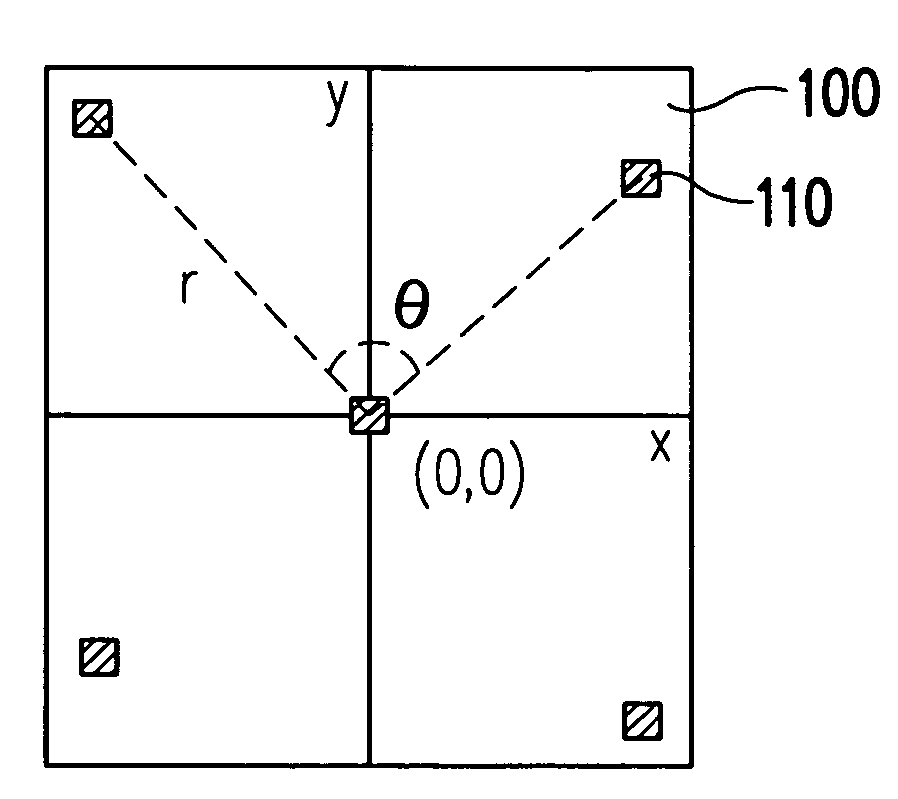
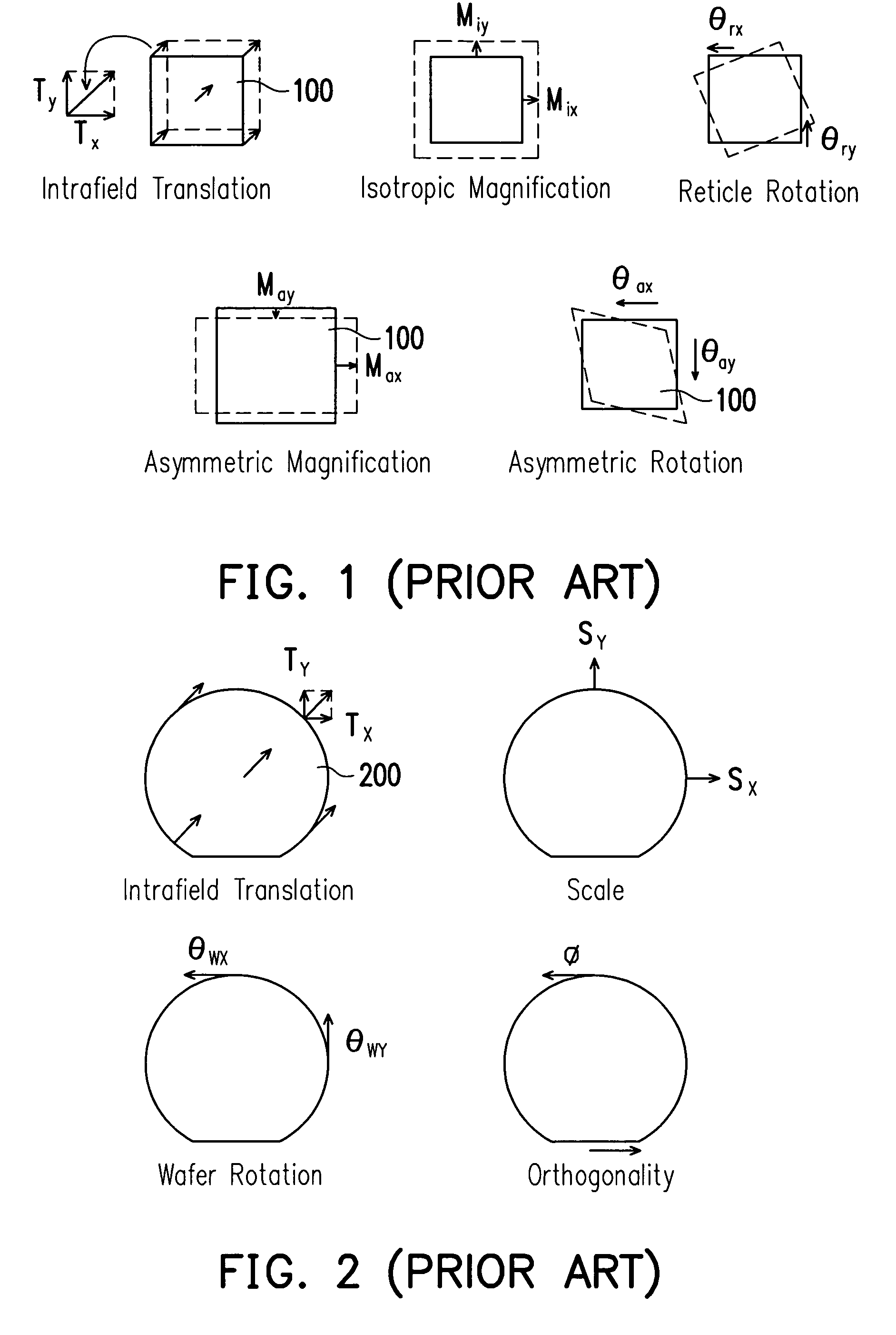
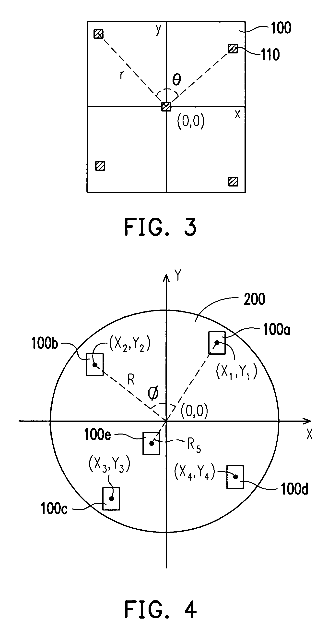
- A new overlay error model and sampling strategy specifically designed for scanner lithography, focusing on nine critical types of intrafield and interfield overlay errors, with an intrafield sampling pattern of 'four corners plus center' and an interfield sampling pattern that includes fields with diverse coordinates and angles, to improve accuracy through least square method fitting.

Semiconductor Industry Standards and Compliance Requirements
The semiconductor industry operates under stringent standards and compliance frameworks that directly impact reticle inspection methodologies for overlay error detection. International standards organizations, including SEMI, ITRS, and IEEE, establish critical specifications that govern inspection accuracy, measurement repeatability, and defect classification protocols. These standards mandate specific overlay tolerance ranges, typically requiring sub-nanometer precision for advanced technology nodes below 7nm, which significantly influences the selection between advanced and conventional inspection techniques.
SEMI standards, particularly SEMI P37 for overlay metrology and SEMI P47 for reticle inspection, define mandatory performance criteria that inspection systems must meet. Advanced reticle inspection systems are increasingly required to comply with tighter specifications, including enhanced sensitivity requirements for detecting overlay errors below 1nm, improved measurement uncertainty protocols, and standardized reporting formats. These compliance requirements often necessitate the adoption of advanced inspection technologies over conventional methods to meet industry benchmarks.
Regulatory compliance extends beyond technical specifications to encompass quality management systems aligned with ISO 9001 and automotive standards like IATF 16949 for semiconductor applications in critical industries. Advanced inspection techniques must demonstrate compliance with statistical process control requirements, including Cpk values exceeding 1.33 for overlay measurements and comprehensive traceability documentation. The FDA's quality system regulations also impact semiconductor inspection processes for medical device applications, requiring validated inspection procedures and documented measurement uncertainty analyses.
International trade regulations and export control requirements, particularly ITAR and EAR classifications, influence the deployment and technology transfer of advanced reticle inspection systems. Compliance with these regulations affects the availability of cutting-edge inspection technologies across different geographical regions and impacts the standardization of inspection methodologies globally. Companies must navigate complex compliance landscapes while maintaining competitive inspection capabilities.
Environmental and safety standards, including RoHS compliance and REACH regulations, impose additional constraints on inspection system design and operation. Advanced reticle inspection systems must incorporate environmentally compliant materials and processes while maintaining performance standards, often driving innovation in inspection technology development to meet both technical and regulatory requirements simultaneously.
SEMI standards, particularly SEMI P37 for overlay metrology and SEMI P47 for reticle inspection, define mandatory performance criteria that inspection systems must meet. Advanced reticle inspection systems are increasingly required to comply with tighter specifications, including enhanced sensitivity requirements for detecting overlay errors below 1nm, improved measurement uncertainty protocols, and standardized reporting formats. These compliance requirements often necessitate the adoption of advanced inspection technologies over conventional methods to meet industry benchmarks.
Regulatory compliance extends beyond technical specifications to encompass quality management systems aligned with ISO 9001 and automotive standards like IATF 16949 for semiconductor applications in critical industries. Advanced inspection techniques must demonstrate compliance with statistical process control requirements, including Cpk values exceeding 1.33 for overlay measurements and comprehensive traceability documentation. The FDA's quality system regulations also impact semiconductor inspection processes for medical device applications, requiring validated inspection procedures and documented measurement uncertainty analyses.
International trade regulations and export control requirements, particularly ITAR and EAR classifications, influence the deployment and technology transfer of advanced reticle inspection systems. Compliance with these regulations affects the availability of cutting-edge inspection technologies across different geographical regions and impacts the standardization of inspection methodologies globally. Companies must navigate complex compliance landscapes while maintaining competitive inspection capabilities.
Environmental and safety standards, including RoHS compliance and REACH regulations, impose additional constraints on inspection system design and operation. Advanced reticle inspection systems must incorporate environmentally compliant materials and processes while maintaining performance standards, often driving innovation in inspection technology development to meet both technical and regulatory requirements simultaneously.
Cost-Benefit Analysis of Advanced vs Conventional Methods
The economic evaluation of advanced reticle inspection systems versus conventional overlay error detection methods reveals significant differences in both initial investment requirements and long-term operational benefits. Advanced inspection technologies, including machine learning-enhanced optical systems and high-resolution electron beam inspection tools, typically require capital investments ranging from $15-25 million per system, compared to $3-8 million for conventional optical inspection equipment. However, this substantial upfront cost differential must be evaluated against the comprehensive operational advantages and yield improvements that advanced systems deliver.
From an operational cost perspective, advanced inspection methods demonstrate superior efficiency through reduced inspection cycle times and enhanced automation capabilities. While conventional techniques may require 2-4 hours for comprehensive reticle inspection with multiple manual verification steps, advanced systems can complete similar inspections in 30-60 minutes with minimal human intervention. This translates to approximately 60-70% reduction in labor costs and significantly improved throughput, particularly critical in high-volume manufacturing environments where inspection bottlenecks directly impact production capacity.
The yield improvement benefits present the most compelling economic argument for advanced inspection adoption. Advanced systems typically achieve 15-25% reduction in overlay-related defect escape rates compared to conventional methods, directly translating to improved wafer yields and reduced rework costs. In advanced node production where individual wafers can cost $15,000-20,000 to process, even marginal yield improvements generate substantial financial returns. Conservative estimates suggest that advanced inspection systems can recover their additional investment costs within 18-24 months through yield improvements alone.
Risk mitigation represents another crucial economic factor, as advanced inspection systems provide enhanced early detection capabilities that prevent costly downstream failures. Conventional methods may miss subtle overlay errors that only manifest as yield losses in final testing, resulting in significant material and processing cost losses. Advanced systems' predictive capabilities and real-time feedback mechanisms reduce these risks substantially, providing additional economic value through improved process stability and reduced scrap rates.
The total cost of ownership analysis over a typical 5-7 year equipment lifecycle consistently favors advanced inspection systems in high-volume production environments, despite higher initial investments, due to their superior operational efficiency, yield contributions, and risk mitigation capabilities.
From an operational cost perspective, advanced inspection methods demonstrate superior efficiency through reduced inspection cycle times and enhanced automation capabilities. While conventional techniques may require 2-4 hours for comprehensive reticle inspection with multiple manual verification steps, advanced systems can complete similar inspections in 30-60 minutes with minimal human intervention. This translates to approximately 60-70% reduction in labor costs and significantly improved throughput, particularly critical in high-volume manufacturing environments where inspection bottlenecks directly impact production capacity.
The yield improvement benefits present the most compelling economic argument for advanced inspection adoption. Advanced systems typically achieve 15-25% reduction in overlay-related defect escape rates compared to conventional methods, directly translating to improved wafer yields and reduced rework costs. In advanced node production where individual wafers can cost $15,000-20,000 to process, even marginal yield improvements generate substantial financial returns. Conservative estimates suggest that advanced inspection systems can recover their additional investment costs within 18-24 months through yield improvements alone.
Risk mitigation represents another crucial economic factor, as advanced inspection systems provide enhanced early detection capabilities that prevent costly downstream failures. Conventional methods may miss subtle overlay errors that only manifest as yield losses in final testing, resulting in significant material and processing cost losses. Advanced systems' predictive capabilities and real-time feedback mechanisms reduce these risks substantially, providing additional economic value through improved process stability and reduced scrap rates.
The total cost of ownership analysis over a typical 5-7 year equipment lifecycle consistently favors advanced inspection systems in high-volume production environments, despite higher initial investments, due to their superior operational efficiency, yield contributions, and risk mitigation capabilities.
Unlock deeper insights with PatSnap Eureka Quick Research — get a full tech report to explore trends and direct your research. Try now!
Generate Your Research Report Instantly with AI Agent
Supercharge your innovation with PatSnap Eureka AI Agent Platform!