Analysis of Chemical Vapor Deposition Parameters in SiC Growth
SEP 28, 20259 MIN READ
Generate Your Research Report Instantly with AI Agent
Patsnap Eureka helps you evaluate technical feasibility & market potential.
SiC CVD Technology Evolution and Objectives
Silicon Carbide (SiC) Chemical Vapor Deposition (CVD) technology has evolved significantly since its inception in the early 1970s. Initially developed as a specialized process for niche applications, SiC CVD has transformed into a critical manufacturing technology for power electronics, optoelectronics, and high-temperature semiconductor devices. The evolution trajectory shows a clear shift from laboratory-scale experimentation to industrial-scale production, with substantial improvements in crystal quality, growth rate, and process control.
The fundamental principle of SiC CVD involves the reaction of silicon and carbon-containing precursor gases at elevated temperatures to form solid SiC on a substrate surface. Early systems utilized simple hot-wall reactors with limited temperature control and precursor delivery capabilities, resulting in films with high defect densities and inconsistent properties. The 1990s marked a turning point with the introduction of more sophisticated reactor designs and improved process monitoring techniques.
Recent technological advancements have focused on addressing key challenges in SiC epitaxial growth, including basal plane dislocations, step-bunching phenomena, and polytype stability. Modern SiC CVD systems incorporate advanced features such as multi-zone heating, precise gas flow control, in-situ monitoring capabilities, and automated process control algorithms. These improvements have enabled the growth of high-quality SiC epitaxial layers with controlled doping profiles and minimal defects.
The primary objectives of current SiC CVD technology development include increasing growth rates while maintaining crystal quality, reducing process costs, enabling larger wafer diameters, and improving uniformity across the wafer surface. Achieving these objectives requires a comprehensive understanding of the complex interplay between various deposition parameters, including temperature gradients, gas flow dynamics, precursor chemistry, and surface kinetics.
Another critical goal is the reduction of specific defects that limit device performance, such as triangular defects, carrots, and downfalls. These defects originate from various sources including substrate imperfections, process instabilities, and gas-phase nucleation events. Developing strategies to minimize these defects while maintaining economically viable growth rates represents a significant technical challenge.
The technology roadmap for SiC CVD aims to support the transition to 200mm and eventually 300mm wafer platforms, which necessitates fundamental redesigns of reactor geometry and process parameters. Additionally, there is growing interest in developing specialized CVD processes for novel SiC-based devices, including MOSFET structures, Schottky diodes, and heterojunction devices that leverage the unique properties of different SiC polytypes.
Market Applications and Demand for SiC Materials
Silicon carbide (SiC) materials have witnessed exponential growth in market demand across multiple industries due to their exceptional properties. The power electronics sector represents the largest market for SiC, with applications in electric vehicles, renewable energy systems, and industrial power supplies. The global SiC power semiconductor market reached approximately $1.4 billion in 2022 and is projected to grow at a CAGR of 34% through 2028, primarily driven by the automotive sector's transition to electric mobility.
In the automotive industry, SiC-based power modules enable higher efficiency in electric vehicle inverters, resulting in extended driving range, faster charging capabilities, and reduced cooling requirements. Major automotive manufacturers including Tesla, BMW, and Toyota have already incorporated SiC power devices in their latest EV models, signaling strong industry adoption.
The renewable energy sector constitutes another significant market for SiC materials, particularly in solar inverters and wind power systems. SiC-based power devices allow for higher switching frequencies and reduced energy losses, improving overall system efficiency by 2-3% compared to traditional silicon-based solutions. This efficiency gain translates to substantial energy savings over the lifetime of renewable energy installations.
Aerospace and defense applications represent a premium market segment for SiC materials, where reliability under extreme conditions is paramount. SiC components are increasingly utilized in radar systems, satellite communications, and aircraft power management systems due to their radiation hardness and high-temperature stability.
The telecommunications infrastructure market has emerged as a growth area for SiC, particularly with the global rollout of 5G networks. Base stations equipped with SiC power amplifiers demonstrate improved energy efficiency and reduced cooling requirements, addressing key operational challenges in network deployment.
Industrial applications including motor drives, uninterruptible power supplies, and high-temperature sensors continue to adopt SiC technology to achieve higher power density and operational efficiency. The industrial automation sector specifically values SiC for enabling more compact and reliable control systems.
Regional market analysis indicates that Asia-Pacific, particularly China, Japan, and South Korea, represents the largest and fastest-growing market for SiC materials, followed by North America and Europe. Government initiatives promoting electric vehicles and renewable energy in these regions further accelerate market growth. Supply chain constraints remain a challenge, with manufacturers investing heavily in expanding SiC wafer production capacity to meet the surging demand across these diverse application sectors.
Current CVD Challenges in SiC Crystal Growth
Chemical Vapor Deposition (CVD) for Silicon Carbide (SiC) growth faces several significant technical challenges that impede the widespread commercialization and application of high-quality SiC devices. The primary challenge lies in controlling the gas-phase nucleation during the deposition process, which often leads to homogeneous nucleation in the gas phase rather than the desired heterogeneous nucleation on the substrate surface. This results in particulate formation and subsequent defects in the grown crystal.
Temperature management presents another critical challenge, as SiC CVD typically requires temperatures exceeding 1500°C. Maintaining uniform temperature distribution across large-diameter substrates remains problematic, leading to thickness variations and polytype inconsistencies in the grown material. Even minor temperature fluctuations can trigger unwanted polytype transitions, particularly between 4H-SiC and 6H-SiC, compromising the electrical properties of the resulting material.
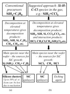
Precursor chemistry optimization continues to challenge researchers, with the traditional silane (SiH4) and propane (C3H8) combination presenting safety concerns and control difficulties. Alternative precursors like methyltrichlorosilane (CH3SiCl3) offer improved safety profiles but introduce new complexities in process parameter optimization and may contribute to chlorine incorporation in the grown layers.
Defect management remains perhaps the most persistent challenge in SiC CVD. Basal plane dislocations (BPDs), threading screw dislocations (TSDs), and threading edge dislocations (TEDs) propagate from the substrate into the epitaxial layers, degrading device performance. Carrot defects, triangular defects, and step-bunching phenomena further complicate the growth of device-quality material, particularly for high-voltage applications requiring thick drift layers.
Scaling to larger wafer diameters (currently transitioning from 150mm to 200mm) introduces additional complexities in maintaining growth uniformity and reducing edge effects. The hot-wall CVD reactors commonly used for SiC epitaxy face significant engineering challenges when scaled to accommodate larger substrates while maintaining thermal uniformity and precursor distribution.
Doping control presents another significant challenge, particularly for achieving precise and uniform n-type and p-type doping profiles. Nitrogen incorporation for n-type doping shows strong crystallographic orientation dependence, while aluminum and boron for p-type doping suffer from memory effects and diffusion issues at high growth temperatures.
The economic viability of SiC CVD processes remains constrained by low growth rates (typically 5-15 μm/h), high energy consumption, and expensive precursor materials. These factors contribute to the overall high cost of SiC devices compared to silicon alternatives, limiting market penetration despite the superior material properties.
Temperature management presents another critical challenge, as SiC CVD typically requires temperatures exceeding 1500°C. Maintaining uniform temperature distribution across large-diameter substrates remains problematic, leading to thickness variations and polytype inconsistencies in the grown material. Even minor temperature fluctuations can trigger unwanted polytype transitions, particularly between 4H-SiC and 6H-SiC, compromising the electrical properties of the resulting material.
Precursor chemistry optimization continues to challenge researchers, with the traditional silane (SiH4) and propane (C3H8) combination presenting safety concerns and control difficulties. Alternative precursors like methyltrichlorosilane (CH3SiCl3) offer improved safety profiles but introduce new complexities in process parameter optimization and may contribute to chlorine incorporation in the grown layers.
Defect management remains perhaps the most persistent challenge in SiC CVD. Basal plane dislocations (BPDs), threading screw dislocations (TSDs), and threading edge dislocations (TEDs) propagate from the substrate into the epitaxial layers, degrading device performance. Carrot defects, triangular defects, and step-bunching phenomena further complicate the growth of device-quality material, particularly for high-voltage applications requiring thick drift layers.
Scaling to larger wafer diameters (currently transitioning from 150mm to 200mm) introduces additional complexities in maintaining growth uniformity and reducing edge effects. The hot-wall CVD reactors commonly used for SiC epitaxy face significant engineering challenges when scaled to accommodate larger substrates while maintaining thermal uniformity and precursor distribution.
Doping control presents another significant challenge, particularly for achieving precise and uniform n-type and p-type doping profiles. Nitrogen incorporation for n-type doping shows strong crystallographic orientation dependence, while aluminum and boron for p-type doping suffer from memory effects and diffusion issues at high growth temperatures.
The economic viability of SiC CVD processes remains constrained by low growth rates (typically 5-15 μm/h), high energy consumption, and expensive precursor materials. These factors contribute to the overall high cost of SiC devices compared to silicon alternatives, limiting market penetration despite the superior material properties.
Parametric Analysis of Modern SiC CVD Processes
01 Temperature control in CVD for SiC growth
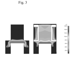
Temperature is a critical parameter in Chemical Vapor Deposition (CVD) for silicon carbide growth. Precise temperature control affects crystal quality, growth rate, and polytype formation. Optimal temperature ranges typically between 1400-1600°C for high-quality SiC epitaxial layers. Temperature gradients within the reactor must be carefully managed to ensure uniform deposition and prevent defects in the crystal structure.- Temperature and pressure control in SiC CVD growth: Temperature and pressure are critical parameters in Chemical Vapor Deposition (CVD) of silicon carbide (SiC). Optimal temperature ranges typically between 1400-1600°C, while pressure can vary from low pressure to atmospheric conditions depending on the desired crystal quality. These parameters significantly influence the growth rate, polytype formation, and defect density in SiC crystals. Precise control of these parameters enables the growth of high-quality SiC substrates with minimal defects.
- Precursor gas composition and flow rates: The composition and flow rates of precursor gases play a crucial role in SiC CVD growth. Common precursors include silane (SiH4) or other silicon-containing gases combined with hydrocarbons like propane (C3H8) or methane (CH4) as carbon sources. The Si/C ratio in the gas phase significantly affects the stoichiometry and quality of the grown SiC layers. Carrier gases such as hydrogen or helium are used to transport the precursors and influence the growth dynamics. Optimizing gas flow rates and ratios is essential for achieving uniform deposition and controlling the growth rate.
- Substrate preparation and orientation effects: Proper substrate preparation is fundamental for successful SiC epitaxial growth by CVD. Surface treatments including polishing, etching, and cleaning significantly impact the quality of the deposited layers. The crystallographic orientation of the substrate (commonly 4H or 6H SiC) determines the polytype and properties of the grown material. Off-axis cut substrates with specific misorientation angles are often used to promote step-flow growth and reduce defects. The substrate temperature distribution and rotation during deposition also affect the uniformity and quality of the grown SiC layers.
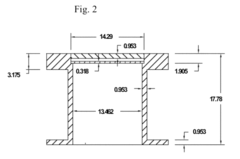
- Reactor design and geometry optimization: The design and geometry of the CVD reactor significantly influence SiC growth parameters and outcomes. Hot-wall and cold-wall reactor configurations offer different advantages for temperature distribution and precursor decomposition. The positioning of gas inlets, susceptor design, and thermal gradients within the reactor chamber affect growth uniformity and efficiency. Optimized reactor geometry helps minimize parasitic deposition, improve precursor utilization, and enhance the quality of SiC crystals. Advanced reactor designs incorporate features for in-situ monitoring and precise control of the growth environment.
- Doping control and impurity management: Controlling doping levels and managing impurities are essential aspects of SiC CVD growth. Intentional doping with nitrogen (n-type) or aluminum (p-type) is achieved by introducing specific gases like nitrogen or trimethylaluminum during deposition. The concentration and distribution of dopants are controlled through precursor flow rates and growth conditions. Minimizing unintentional impurities such as oxygen and transition metals is crucial for achieving high-quality SiC with desired electrical properties. Post-growth treatments may be employed to activate dopants or reduce defects in the crystal structure.
02 Precursor gas composition and flow rates
The composition and flow rates of precursor gases significantly impact SiC growth in CVD processes. Common precursors include silane (SiH4) or other silicon-containing gases combined with hydrocarbons like propane (C3H8) or methane (CH4). The Si/C ratio in the gas phase is crucial for controlling polytype formation and reducing defects. Carrier gases such as hydrogen or argon help transport the precursors and influence the deposition kinetics. Optimizing flow rates and gas ratios is essential for achieving high-quality SiC crystal growth.Expand Specific Solutions03 Pressure parameters and reactor design
Reactor pressure is a key parameter affecting SiC growth during CVD. Low-pressure CVD (typically 100-300 Torr) offers better control over film uniformity and quality, while atmospheric pressure processes may provide higher growth rates. The reactor design, including geometry, gas inlet configuration, and substrate positioning, significantly influences gas flow dynamics and temperature distribution. These factors directly impact growth uniformity, efficiency, and defect density in the resulting SiC crystals.Expand Specific Solutions04 Substrate preparation and orientation
Substrate preparation and crystallographic orientation play crucial roles in SiC epitaxial growth by CVD. Surface treatments such as hydrogen etching, chemical cleaning, or in-situ thermal preparation help remove surface contaminants and create optimal nucleation sites. The substrate orientation (commonly off-axis cuts of 4° or 8° from the basal plane) influences polytype stability, step-flow growth mechanisms, and defect propagation. Proper substrate preparation minimizes defects and ensures high-quality epitaxial layers with controlled doping profiles.Expand Specific Solutions05 Growth rate control and doping techniques
Controlling growth rate and incorporating dopants are essential aspects of SiC CVD processes. Growth rates typically range from 5-100 μm/h depending on application requirements, with slower rates generally yielding higher quality crystals. Intentional doping is achieved by introducing gases like nitrogen (n-type) or aluminum-containing precursors (p-type) during growth. The concentration and distribution of dopants are controlled by adjusting gas flow rates, temperature, and pressure. Advanced techniques include step-controlled epitaxy and site-competition epitaxy to manage doping efficiency and crystal quality simultaneously.Expand Specific Solutions
Leading Manufacturers and Research Institutions
The Chemical Vapor Deposition (CVD) for SiC growth market is currently in a growth phase, with increasing adoption driven by demand for wide bandgap semiconductors in power electronics and electric vehicles. The global SiC market is projected to reach approximately $3-4 billion by 2025, with CVD processes representing a critical manufacturing component. Technologically, the field shows varying maturity levels across players. Industry leaders like Wolfspeed and Coherent Corp. have established advanced CVD parameter control for high-quality SiC epitaxy, while emerging companies such as SICC, Dongguan TIANYU, and Pallidus are rapidly advancing their capabilities. Regional competition is intensifying with Chinese manufacturers (Jingyue Semiconductor, Qinghe Jingyuan) expanding capacity, while established players in Japan (RESONAC) and Europe (SGL Carbon) focus on process refinement and specialized applications.
Coherent Corp.
Technical Solution: Coherent Corp. (formerly II-VI) has developed a specialized CVD approach for SiC epitaxial growth focusing on precision-controlled gas flow dynamics and temperature uniformity. Their technology employs a horizontal hot-wall reactor design with advanced thermal management systems that maintain temperature variations below ±2°C across the growth zone. The company utilizes silane and propane precursors with hydrogen carrier gas, but has innovated with proprietary gas injection systems that optimize precursor decomposition and species transport to the substrate surface. Coherent's process achieves growth rates of 8-12 μm/h while maintaining excellent doping uniformity (±10%) across 150mm wafers. Their technology incorporates real-time optical monitoring systems that allow for in-situ assessment of growth parameters, enabling dynamic adjustments during the deposition process to optimize crystal quality and reduce defects like triangular defects and step-bunching that commonly occur in SiC epitaxy.
Strengths: Superior temperature uniformity control leading to consistent wafer quality; integrated real-time monitoring capabilities; excellent doping precision across large wafers. Weaknesses: Moderate growth rates compared to some competitors; complex reactor maintenance requirements; higher initial capital investment for their advanced monitoring systems.
SICC Co., Ltd.
Technical Solution: SICC Co. has developed a specialized CVD technology for SiC crystal growth that focuses on high-purity material production. Their approach utilizes a vertical hot-wall reactor design operating at temperatures between 1500-1700°C with precisely controlled temperature gradients to minimize thermal stress. SICC's process employs silane (SiH4) and ethylene (C2H4) as precursors with ultra-high purity hydrogen as carrier gas, achieving growth rates of 6-10 μm/h. A distinguishing feature of their technology is the implementation of a two-stage growth process: an initial low-temperature nucleation layer followed by high-temperature main growth, which significantly reduces stacking faults and micropipes. SICC has also developed proprietary substrate preparation techniques involving in-situ hydrogen etching and surface reconstruction steps that improve epitaxial layer adhesion and reduce interface defects. Their process achieves doping concentration control within ±15% across 100mm and 150mm substrates, with particular expertise in producing semi-insulating SiC materials with resistivity exceeding 1×10^9 Ω·cm.
Strengths: Exceptional material purity suitable for high-voltage applications; specialized expertise in semi-insulating SiC production; effective defect management through two-stage growth process. Weaknesses: Lower growth rates compared to industry leaders; limited to smaller diameter wafers; higher production costs due to extended process duration and stringent purity requirements.
Critical Patents and Breakthroughs in SiC Deposition
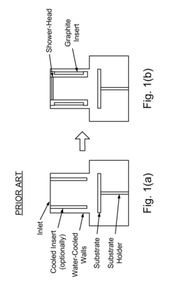
Method for the growth of SiC, by chemical vapor deposition, using precursors in modified cold-wall reactor
PatentActiveUS8329252B2
Innovation
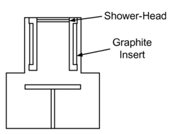
- Incorporating a refractory insert and showerhead in the reactor design to enhance temperature uniformity, and using halogenated carbon precursors with specific silicon-to-carbon and silicon-to-chlorine ratios to increase growth rates and suppress parasitic deposits, allowing for SiC growth at lower temperatures.
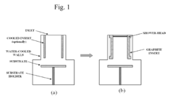
Method, system, and apparatus for the growth of SiC and related or similar material, by chemical vapor deposition, using precursors in modified cold-wall reactor
PatentActiveUS7901508B2
Innovation
- The introduction of a refractory insert and a showerhead unit in the reactor design, along with the use of halogenated carbon precursors and chlorine-containing species to optimize silicon-to-carbon and silicon-to-chlorine ratios, enhances temperature uniformity, suppresses silicon nucleation, and increases the SiC growth rate while maintaining high layer quality at lower temperatures.
Environmental Impact and Sustainability Considerations
The chemical vapor deposition (CVD) process for silicon carbide (SiC) growth, while technologically advanced, presents significant environmental challenges that warrant careful consideration. The process typically involves the use of hazardous precursor gases such as silane (SiH4) and various hydrocarbon sources, which can contribute to air pollution if not properly managed. Additionally, the high-temperature operations required for SiC deposition (typically 1500-2000°C) result in substantial energy consumption, contributing to the carbon footprint of semiconductor manufacturing facilities.
Waste management represents another critical environmental concern in SiC CVD processes. The deposition chambers require regular cleaning to remove unwanted deposits, often using perfluorinated compounds (PFCs) or nitrogen trifluoride (NF3), which are potent greenhouse gases with global warming potentials thousands of times greater than CO2. The semiconductor industry has recognized these challenges and has been implementing abatement systems to reduce emissions, though their effectiveness varies considerably across facilities.
Water usage in cooling systems and post-deposition cleaning processes also presents sustainability challenges. A typical semiconductor fabrication facility may consume millions of gallons of ultra-pure water daily, with SiC production contributing significantly to this demand. The contaminated wastewater often contains trace amounts of toxic materials that require specialized treatment before discharge.
Recent sustainability initiatives in SiC CVD technology have focused on several promising directions. Process optimization through precise parameter control has demonstrated potential for reducing precursor gas consumption by 15-20% while maintaining growth quality. Advanced reactor designs incorporating improved gas flow dynamics have shown up to 30% reduction in energy requirements. Additionally, closed-loop systems for precursor recycling are being developed, potentially reducing both waste generation and raw material consumption.
The economic benefits of environmentally optimized SiC CVD processes are increasingly recognized. Companies implementing sustainable practices report reduced operational costs through energy savings, decreased waste disposal expenses, and lower regulatory compliance costs. Furthermore, as environmental regulations tighten globally, manufacturers with established sustainable practices gain competitive advantages in terms of market access and corporate reputation.
Looking forward, the industry is exploring alternative precursors with lower environmental impact and developing ambient-temperature catalytic processes that could dramatically reduce energy requirements. These innovations, coupled with broader adoption of renewable energy sources for powering CVD facilities, present a pathway toward significantly more sustainable SiC production methodologies in the coming decade.
Quality Control and Characterization Methods
Quality control and characterization methods are critical components in the SiC growth process using Chemical Vapor Deposition (CVD). The industry has developed sophisticated techniques to ensure consistent material quality and performance characteristics. These methods can be broadly categorized into in-situ monitoring techniques and post-growth characterization approaches.
In-situ monitoring during CVD growth provides real-time feedback on process parameters and growing crystal quality. Optical emission spectroscopy (OES) enables monitoring of gas-phase species concentrations, helping operators maintain optimal precursor ratios. Laser reflectance techniques measure growth rates with high precision, allowing for immediate process adjustments. Temperature mapping using infrared pyrometry ensures uniform thermal conditions across the substrate, critical for minimizing defect formation.
Post-growth characterization encompasses physical, chemical, and electrical property assessments. X-ray diffraction (XRD) techniques reveal crystallographic information, including polytype determination, lattice parameters, and strain analysis. Scanning electron microscopy (SEM) and atomic force microscopy (AFM) provide surface morphology data at different scales, identifying step bunching, micropipes, and other surface defects that impact device performance.
Electrical characterization methods include Hall effect measurements for carrier concentration and mobility determination. Capacitance-voltage (C-V) profiling reveals doping distributions, while deep-level transient spectroscopy (DLTS) identifies electrically active defects. These measurements directly correlate with device performance and reliability, making them essential quality indicators.
Defect-specific characterization techniques have gained prominence as SiC applications become more demanding. Photoluminescence spectroscopy identifies specific point defects, while transmission electron microscopy (TEM) reveals extended defects like dislocations and stacking faults. Etching techniques using molten KOH have become standard for revealing and quantifying dislocations, with defect densities now routinely measured in terms of EPD (etch pit density).
Statistical process control (SPC) methodologies have been implemented to track quality metrics across production runs. Key performance indicators include doping uniformity (typically targeting <5% variation), thickness uniformity (<2% variation), and defect densities (<1000 cm^-2 for modern processes). These metrics are continuously monitored using control charts to identify process drift before specification limits are exceeded.
Advanced characterization techniques continue to emerge, including synchrotron-based X-ray topography for non-destructive defect imaging and Raman spectroscopy for stress and polytype analysis. These methods provide deeper insights into material quality and process optimization pathways, supporting the ongoing advancement of SiC technology for power electronics and other demanding applications.
Unlock deeper insights with Patsnap Eureka Quick Research — get a full tech report to explore trends and direct your research. Try now!
Generate Your Research Report Instantly with AI Agent
Supercharge your innovation with Patsnap Eureka AI Agent Platform!