How Chemical Vapor Deposition Enables Large Area Graphene Synthesis
SEP 28, 202510 MIN READ
Generate Your Research Report Instantly with AI Agent
Patsnap Eureka helps you evaluate technical feasibility & market potential.
Graphene CVD Technology Evolution and Objectives
Graphene, a single layer of carbon atoms arranged in a hexagonal lattice, has emerged as a revolutionary material since its isolation in 2004. The evolution of Chemical Vapor Deposition (CVD) technology for graphene synthesis represents one of the most significant advancements in materials science over the past two decades, transforming graphene from a laboratory curiosity to a commercially viable material.
The journey of CVD graphene synthesis began with rudimentary methods in the early 2000s, primarily focused on small-scale production for research purposes. Initial CVD approaches utilized simple tube furnaces with copper or nickel substrates, producing graphene with inconsistent quality and limited dimensions. These early techniques laid the groundwork for understanding the fundamental growth mechanisms but were inadequate for industrial applications.
By 2010, significant progress had been made in optimizing growth parameters, including temperature profiles, gas compositions, and substrate preparations. Researchers discovered that careful control of carbon precursor gases (typically methane or ethylene) and carrier gases (hydrogen and argon) could dramatically improve graphene quality. The introduction of roll-to-roll CVD processes around 2010-2012 marked a pivotal moment, enabling continuous production of meter-scale graphene films.
The period from 2013 to 2018 saw remarkable advancements in substrate engineering and transfer techniques. Copper foils emerged as the preferred growth substrate due to their low carbon solubility, which promotes surface-catalyzed growth rather than precipitation. Simultaneously, researchers developed improved transfer methods to move graphene from metal substrates to target applications without introducing defects or contamination.
Recent technological evolution (2019-present) has focused on addressing three critical challenges: reducing defect density, enhancing scalability, and lowering production costs. Plasma-enhanced CVD and low-pressure CVD variants have gained prominence for their ability to produce higher-quality graphene at lower temperatures. Additionally, the development of multi-zone CVD systems has enabled precise control over growth conditions across large areas.
The primary objectives driving current CVD graphene research include achieving wafer-scale production of single-crystal graphene, developing direct growth methods on insulating substrates to eliminate transfer steps, and establishing environmentally sustainable synthesis protocols. There is also significant interest in tailoring CVD processes for specialized graphene variants, such as functionalized graphene, doped graphene, and graphene-based heterostructures.
Looking forward, the technology roadmap aims to achieve industrial-scale production of defect-free graphene with customizable properties at economically viable costs. This evolution is expected to catalyze graphene's integration into commercial applications spanning electronics, energy storage, composites, and biomedical devices, potentially revolutionizing multiple industries through the unique properties of this two-dimensional material.
Market Applications and Demand for Large-Area Graphene
The graphene market has witnessed substantial growth in recent years, driven by the material's exceptional properties and expanding applications across multiple industries. Current market analysis indicates that large-area graphene, particularly that produced through Chemical Vapor Deposition (CVD), is experiencing accelerated demand due to its superior quality and scalability advantages over other production methods.
Electronics manufacturers represent the largest market segment for large-area graphene, with applications in flexible displays, touchscreens, and next-generation semiconductors. The consumer electronics sector values CVD graphene for its transparency, conductivity, and mechanical flexibility, which enable thinner, more durable, and energy-efficient devices. Major smartphone and tablet manufacturers have already begun incorporating graphene components into prototype devices, signaling strong future demand.
Energy storage represents another significant market opportunity, with large-area graphene being integrated into advanced battery and supercapacitor technologies. The automotive industry, particularly electric vehicle manufacturers, has shown increasing interest in graphene-enhanced energy storage solutions that offer faster charging times and higher energy densities. This sector's demand is expected to grow substantially as electric vehicle adoption accelerates globally.
The biomedical field has emerged as a promising growth area for large-area graphene applications. Researchers and companies are developing graphene-based biosensors, drug delivery systems, and tissue engineering scaffolds that leverage the material's biocompatibility and large surface area. These applications require high-quality, defect-free graphene sheets that only CVD methods can reliably produce at scale.
Aerospace and defense industries are exploring large-area graphene for lightweight composite materials, electromagnetic shielding, and advanced coatings. The material's strength-to-weight ratio and thermal properties make it particularly valuable for these high-performance applications where material reliability is critical.
Market forecasts suggest that as CVD graphene production techniques continue to mature and costs decrease, new application areas will emerge. The construction industry has begun investigating graphene-enhanced concrete and coatings, while the textile sector is developing smart fabrics incorporating graphene for enhanced durability and functionality.
Regional market analysis shows Asia-Pacific leading in graphene demand, followed by North America and Europe. This distribution aligns with manufacturing centers for electronics and automotive industries, the primary consumers of large-area graphene materials. As production scales and prices decrease, wider industrial adoption is anticipated across global markets.
Current CVD Techniques and Scalability Challenges
Chemical Vapor Deposition (CVD) has emerged as the predominant method for large-scale graphene synthesis, offering significant advantages over mechanical exfoliation techniques. Current CVD approaches primarily utilize transition metal substrates such as copper and nickel as catalytic surfaces for graphene growth. The process typically involves hydrocarbon decomposition at elevated temperatures (800-1000°C) in controlled atmospheric conditions, followed by carbon atom nucleation and crystallization into graphene sheets.
Copper-based CVD represents the most widely adopted technique for monolayer graphene production. The low carbon solubility in copper facilitates surface-mediated growth, resulting in predominantly single-layer graphene with coverage exceeding 95%. This process employs methane as the carbon source and hydrogen as both carrier gas and growth regulator, with precise control of gas ratios being critical for defect minimization.
Nickel-based CVD, conversely, enables multilayer graphene synthesis through a dissolution-precipitation mechanism. The higher carbon solubility in nickel allows carbon atoms to diffuse into the substrate at high temperatures and precipitate during cooling, forming multiple graphene layers. While offering faster growth rates, this approach presents challenges in layer number uniformity across large areas.
Recent advancements include plasma-enhanced CVD (PECVD), which reduces process temperatures to 400-600°C through plasma activation of precursor gases. This development has expanded substrate compatibility to include temperature-sensitive materials, potentially enabling direct integration with semiconductor manufacturing processes. Roll-to-roll CVD represents another significant innovation, allowing continuous graphene production on flexible metal foils at meters-per-minute speeds.
Despite these advances, substantial scalability challenges persist. Maintaining structural uniformity across large areas remains problematic, with defect density and layer consistency deteriorating as substrate dimensions increase. Current industrial-scale processes typically exhibit defect densities of 10^10-10^11 cm^-2, significantly higher than the 10^8-10^9 cm^-2 achieved in laboratory settings.
Transfer processes constitute another major bottleneck, as graphene must be removed from the growth substrate and transferred to target substrates for most applications. Conventional polymer-assisted transfer methods introduce contaminants and structural damage, compromising electrical and mechanical properties. Alternative techniques such as electrochemical delamination show promise but remain challenging to scale reliably.
Energy consumption presents additional concerns, with traditional CVD requiring sustained high temperatures and vacuum conditions. The associated carbon footprint and operational costs limit commercial viability, particularly for consumer electronics applications where cost sensitivity is paramount. Emerging low-temperature CVD variants and catalyst recycling strategies aim to address these efficiency challenges but remain in early development stages.
State-of-the-Art CVD Reactor Designs and Processes
01 CVD process parameters for large-area graphene synthesis
Specific process parameters in Chemical Vapor Deposition (CVD) significantly impact the quality and size of graphene sheets. These parameters include temperature control, gas flow rates, pressure conditions, and reaction time. Optimizing these variables allows for the controlled growth of uniform, large-area graphene films with minimal defects. The precise manipulation of these parameters enables scalable production of high-quality graphene suitable for industrial applications.- CVD process parameters for large-area graphene synthesis: Specific process parameters in Chemical Vapor Deposition (CVD) significantly impact the quality and size of graphene sheets. These parameters include temperature control, gas flow rates, pressure conditions, and reaction time. Optimizing these variables allows for the controlled growth of large-area, high-quality graphene films with uniform thickness and minimal defects. The precise manipulation of these parameters enables scalable production of graphene sheets suitable for industrial applications.
- Substrate selection and preparation for large-area graphene growth: The choice and preparation of substrate materials play a crucial role in large-area graphene synthesis via CVD. Metal substrates such as copper and nickel are commonly used due to their catalytic properties and low carbon solubility. Surface treatment techniques including polishing, annealing, and cleaning are essential to remove contaminants and create optimal conditions for graphene nucleation and growth. Properly prepared substrates enable the formation of continuous, large-area graphene films with improved crystallinity.
- Carbon source selection and delivery methods: The selection of appropriate carbon sources and their delivery methods significantly influences large-area graphene synthesis. Various hydrocarbon precursors such as methane, ethylene, and acetylene can be used, each offering different decomposition characteristics and graphene growth rates. Controlled delivery systems regulate the concentration and flow of these carbon sources into the reaction chamber. Advanced precursor delivery techniques help achieve uniform carbon distribution across large substrates, resulting in homogeneous graphene films with consistent properties.
- Transfer techniques for large-area graphene films: After CVD synthesis, specialized transfer techniques are required to move large-area graphene from the growth substrate to target substrates for various applications. These methods include polymer-assisted transfer using PMMA or PDMS as support layers, roll-to-roll transfer for continuous production, and dry transfer approaches that minimize contamination and damage. Advanced transfer techniques preserve the structural integrity and electrical properties of graphene while enabling its integration into various device architectures and flexible substrates.
- Reactor design and scaling for industrial production: Specialized reactor designs are essential for scaling up CVD graphene synthesis to industrial levels. These include custom-built chambers with precise temperature control zones, uniform gas distribution systems, and large-diameter reaction tubes. Roll-to-roll CVD systems enable continuous production of graphene on flexible substrates. Advanced reactor configurations incorporate in-situ monitoring tools to ensure consistent quality during large-area synthesis. These engineering innovations address challenges in maintaining uniform growth conditions across large substrates, enabling commercial-scale graphene production.
02 Substrate selection and preparation for large-area graphene growth
The choice and preparation of substrate materials play a crucial role in large-area graphene synthesis via CVD. Metal substrates such as copper and nickel are commonly used due to their catalytic properties and ability to support continuous graphene growth. Surface preparation techniques including polishing, annealing, and cleaning are essential to remove contaminants and create optimal conditions for uniform graphene nucleation and growth across large areas.Expand Specific Solutions03 Precursor gas composition and delivery systems
The composition and delivery method of precursor gases significantly influence large-area graphene synthesis. Carbon-containing gases such as methane, ethylene, or acetylene serve as carbon sources, while hydrogen and argon are used as carrier and reducing gases. Advanced gas delivery systems with precise flow control enable uniform distribution of precursors across large substrate areas, resulting in homogeneous graphene growth. The ratio of carbon source to other gases and their introduction timing are critical factors affecting graphene quality and coverage.Expand Specific Solutions04 Transfer techniques for large-area graphene films
After CVD synthesis, transferring large-area graphene films from growth substrates to target substrates while maintaining structural integrity is challenging. Various transfer methods have been developed, including polymer-assisted transfer using PMMA or PDMS, roll-to-roll transfer for continuous processing, and dry transfer techniques. These methods aim to minimize damage, contamination, and wrinkles in the graphene film during transfer, which is crucial for preserving the electrical, mechanical, and optical properties of large-area graphene sheets.Expand Specific Solutions05 Reactor design and scaling for industrial production
Specialized reactor designs are essential for scaling up graphene CVD synthesis from laboratory to industrial scale. These designs focus on maintaining uniform temperature distribution, gas flow dynamics, and pressure conditions across large reaction chambers. Innovations include roll-to-roll continuous CVD systems, multi-zone heating arrangements, and customized gas shower heads for even precursor distribution. Advanced monitoring and control systems enable real-time process adjustment to ensure consistent quality during large-area graphene production.Expand Specific Solutions
Leading Companies and Research Institutions in CVD Graphene
Chemical Vapor Deposition (CVD) for large area graphene synthesis is currently in a growth phase, with the global market expanding rapidly due to increasing applications in electronics, energy storage, and composites. The market is projected to reach significant scale as graphene transitions from research to commercial applications. Technologically, CVD methods are maturing but still evolving, with key players demonstrating varying levels of expertise. Academic institutions like Peking University, Chinese Academy of Sciences, and The University of Manchester lead fundamental research, while companies including Bluestone Global Tech, Applied Materials, and Global Graphene Group focus on scaling production technologies. Huawei and Lockheed Martin represent end-users developing application-specific implementations. The ecosystem shows a collaborative dynamic between research institutions advancing fundamental science and commercial entities working toward industrial-scale production.
Peking University
Technical Solution: Peking University has developed a sophisticated CVD approach for large-area graphene synthesis called "Confined-Flow CVD" (CF-CVD). Their technology utilizes a specially designed reactor with controlled gas flow dynamics that create laminar flow patterns across the growth substrate. This confined flow system enables precise control over the local concentration of carbon precursors and carrier gases throughout the growth process. The university's researchers have optimized a two-stage growth protocol where initial nucleation occurs under low carbon concentration conditions followed by a controlled growth phase with increased precursor flow [5]. This approach produces large single-crystal graphene domains exceeding 500 μm in diameter that merge to form continuous films with minimal grain boundaries. Peking University has also pioneered low-pressure CVD techniques that operate at pressures below 100 Pa, which enhances surface diffusion of carbon species and promotes more uniform graphene formation. Their system incorporates rapid thermal control mechanisms that allow precise temperature ramping profiles, critical for controlling nucleation density and growth rates. The university has developed specialized copper substrate pretreatment methods involving electropolishing and annealing steps that create atomically smooth surfaces with preferred crystallographic orientations, significantly improving graphene quality. Their process can produce graphene films with carrier mobilities exceeding 15,000 cm²/Vs and defect densities below 2×10¹⁰ cm⁻² across 12-inch substrates, demonstrating excellent scalability while maintaining high quality.
Strengths: Exceptional control over graphene crystal size and orientation; strong fundamental understanding of growth mechanisms supported by advanced characterization capabilities; established collaborations with Chinese semiconductor manufacturers for technology transfer. Weaknesses: Their high-quality growth process requires ultra-high purity gases and precisely controlled environments that increase production costs; the technology still faces challenges with efficient transfer of large-area graphene to target substrates.
GLOBAL GRAPHENE GROUP INC
Technical Solution: Global Graphene Group has developed a proprietary CVD process called "Continuous Flow CVD" (CF-CVD) specifically optimized for industrial-scale graphene production. Their technology employs a specialized reactor design that allows for continuous graphene growth on metal foils (primarily copper) that can be fed through the system in a roll-to-roll configuration. The process utilizes carefully controlled methane and hydrogen gas mixtures with precise thermal management across multiple heating zones to ensure uniform nucleation and growth of high-quality graphene films [3]. Their CVD system incorporates rapid cooling mechanisms to minimize carbon precipitation during the cooling phase, which significantly reduces multilayer formation and defects. The company has developed specialized catalyst pretreatment methods that enhance copper grain size and orientation, leading to larger graphene domains with fewer grain boundaries. Global Graphene Group's technology also features an integrated transfer system that uses temporary polymer supports and electrochemical delamination to separate graphene from growth substrates with minimal damage. Their process can produce graphene sheets with consistently high carrier mobility (>15,000 cm²/Vs) and optical transparency (>97%) at production speeds reaching several meters per minute, making it suitable for commercial applications in electronics, energy storage, and composite materials.
Strengths: Vertically integrated business model covering the entire value chain from graphene production to application development; strong patent portfolio with over 500 patents; established commercial production capacity. Weaknesses: Their CVD process still faces challenges with cost-effectiveness at very large scales; the transfer process remains a bottleneck for certain high-performance applications requiring pristine graphene.
Breakthrough Patents in Large-Area Graphene Synthesis
Graphene synthesis by suppressing evaporative substrate loss during low pressure chemical vapor deposition
PatentWO2015038267A3
Innovation
- Configuring the substrate as a tube prior to exposure to organic compounds at high temperature to suppress evaporative substrate loss during low pressure CVD.
- Using a low flow rate of gaseous carbon source initially, followed by increased flow rate after the nucleation period to optimize large single-crystal graphene growth.
- Suppression of evaporative substrate loss as a novel approach to enable large single-crystal graphene film synthesis in low pressure CVD environments.
Method for using carbon source having multiple benzene rings to grow graphene over large area by chemical vapor deposition at low temperature
PatentWO2013104141A1
Innovation
- Using polyphenyl aromatic hydrocarbons as the carbon source, graphene is grown on the surface of the copper foil through low-temperature chemical vapor deposition, and the decomposition rate of the carbon source is controlled through the carbon source decomposition method or spin coating method to achieve controllable number of layers. And transfer the graphene to the flexible substrate.
Material Characterization and Quality Control Methods
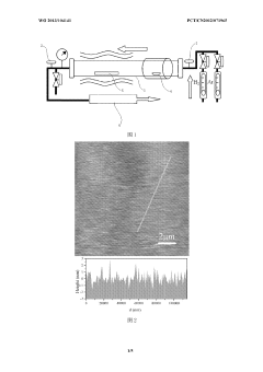
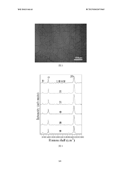
The quality assessment of graphene synthesized through Chemical Vapor Deposition (CVD) requires sophisticated characterization techniques to ensure consistency across large areas. Raman spectroscopy stands as the primary non-destructive method for evaluating graphene quality, providing critical information about layer numbers, defect density, and crystalline structure. The characteristic G-band (~1580 cm⁻¹) and 2D-band (~2700 cm⁻¹) peaks, along with their intensity ratio (I₂ᴅ/Iɢ), serve as reliable indicators of graphene layer count, while the presence and intensity of the D-band (~1350 cm⁻¹) quantifies defect concentration.
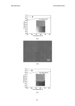
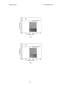
Scanning electron microscopy (SEM) and atomic force microscopy (AFM) complement spectroscopic methods by providing visual confirmation of graphene coverage, uniformity, and surface morphology. SEM offers rapid large-area assessment of graphene continuity and domain boundaries, while AFM delivers precise topographical measurements with nanometer resolution, essential for thickness verification and surface roughness quantification.
Electrical characterization techniques, including Hall effect measurements and four-point probe testing, evaluate carrier mobility, sheet resistance, and conductivity—properties directly linked to graphene quality and performance in electronic applications. These measurements help establish correlations between synthesis parameters and electrical performance, guiding process optimization efforts.
X-ray photoelectron spectroscopy (XPS) provides elemental composition analysis, detecting impurities and functional groups that may compromise graphene properties. This technique proves particularly valuable for identifying residual catalyst particles, oxygen-containing groups, and other contaminants introduced during synthesis or transfer processes.
In-line quality control systems incorporating optical inspection and automated Raman mapping enable real-time monitoring during industrial-scale production. These systems can detect variations in layer uniformity, identify defects, and trigger process adjustments before significant material waste occurs. Statistical process control methodologies applied to characterization data help establish acceptable quality thresholds and identify process drift.
Transmission electron microscopy (TEM) offers atomic-resolution imaging of graphene's lattice structure, providing definitive confirmation of crystalline quality and layer count. While too time-intensive for routine quality control, TEM serves as the gold standard for validating other characterization methods and investigating unusual defect structures or growth anomalies.
Standardized testing protocols combining multiple characterization techniques ensure comprehensive quality assessment across different production batches. These protocols typically include sampling strategies that balance throughput requirements with statistical confidence, enabling meaningful comparisons between different CVD systems and process parameters.
Sustainability and Cost Analysis of Industrial-Scale Production
The industrial-scale production of graphene via Chemical Vapor Deposition (CVD) presents significant sustainability challenges and cost considerations that must be carefully evaluated. Current CVD processes for large-area graphene synthesis typically require high temperatures (800-1000°C) and energy-intensive operations, resulting in substantial carbon footprints. Energy consumption represents approximately 45-60% of the total production costs, making energy efficiency improvements critical for both environmental and economic viability.
Material utilization efficiency in industrial CVD processes remains suboptimal, with precursor gas utilization rates often below 30%. The primary precursors—methane and hydrogen—contribute to greenhouse gas emissions when not fully utilized, while copper substrates, despite being recyclable, involve energy-intensive recovery processes. Advanced precursor recovery systems could potentially reduce waste by 40-50%, significantly improving the sustainability profile.
Water usage presents another environmental concern, particularly for cooling systems and substrate cleaning processes. Industrial-scale operations can consume 15-20 liters of water per square meter of graphene produced. Implementing closed-loop water recycling systems could reduce consumption by up to 80%, though requiring additional capital investment of approximately $200,000-500,000 per production line.
From a cost perspective, current industrial-scale CVD graphene production ranges from $50-200 per square meter, depending on quality requirements and production volume. Capital expenditure for establishing a production facility with 10,000 m²/year capacity typically requires $5-10 million investment. Operational costs are dominated by energy (45-60%), materials (20-30%), labor (10-15%), and maintenance (5-10%).
Economic viability improves significantly with scale, as unit costs can decrease by 30-40% when production volumes increase tenfold. However, market adoption remains the critical factor determining return on investment. Current payback periods range from 3-7 years depending on production scale and market penetration.
Recent innovations in catalyst reuse and roll-to-roll processing show promise for reducing both environmental impact and production costs. Continuous production methods could potentially reduce energy consumption by 25-35% while increasing throughput by 300-500%. Additionally, alternative catalysts and lower-temperature processes under development may further improve the sustainability profile of industrial graphene production.
For long-term sustainability, life cycle assessment studies indicate that graphene's environmental benefits in end applications (such as energy storage, lightweight materials, and water filtration) may offset production impacts if production methods continue to improve and applications achieve widespread adoption.
Unlock deeper insights with Patsnap Eureka Quick Research — get a full tech report to explore trends and direct your research. Try now!
Generate Your Research Report Instantly with AI Agent
Supercharge your innovation with Patsnap Eureka AI Agent Platform!