Comparative Study of Plasma Enhanced vs Thermal Chemical Vapor Deposition
SEP 28, 20259 MIN READ
Generate Your Research Report Instantly with AI Agent
Patsnap Eureka helps you evaluate technical feasibility & market potential.
CVD Technology Background and Objectives
Chemical Vapor Deposition (CVD) technology has evolved significantly since its inception in the late 19th century, with major industrial applications emerging in the 1960s. The technology fundamentally involves the deposition of solid materials onto substrates through chemical reactions of vapor-phase precursors. This process has become instrumental in semiconductor manufacturing, optical coatings, and advanced materials development.
The evolution of CVD technology has followed the increasing demands for precision, efficiency, and versatility in material deposition processes. Traditional thermal CVD, which relies on heat to activate chemical reactions, has been the foundation of this technology. However, the introduction of plasma enhancement in the 1970s marked a significant advancement, allowing for lower temperature processing and expanded material capabilities.
Current technological trends in CVD are moving toward more precise control of film properties, reduced environmental impact, and integration with other manufacturing processes. The industry is witnessing a shift toward atomic-level precision, with techniques such as Atomic Layer Deposition (ALD) gaining prominence as an extension of CVD principles.
The primary objective of comparing Plasma Enhanced Chemical Vapor Deposition (PECVD) with Thermal CVD is to comprehensively understand their respective advantages, limitations, and optimal application scenarios. This comparison aims to provide insights into how these technologies can be leveraged for specific material requirements, energy efficiency considerations, and production scale demands.
PECVD utilizes electrical energy to generate plasma, which creates reactive species at lower temperatures than would be possible with thermal energy alone. This enables deposition on temperature-sensitive substrates and offers unique film properties. Conversely, thermal CVD provides excellent film uniformity and is often simpler to implement and scale.
The technological goals of this comparative study include identifying the critical parameters affecting deposition quality, understanding the fundamental mechanisms of each process, and exploring hybrid approaches that might combine the benefits of both methods. Additionally, the study seeks to map the future trajectory of these technologies in light of emerging applications in nanotechnology, renewable energy, and advanced electronics.
By establishing a clear understanding of the historical context, current capabilities, and future potential of both PECVD and thermal CVD, this study aims to guide strategic decisions in research, development, and industrial implementation of these critical deposition technologies.
Market Applications and Industry Demand
The Chemical Vapor Deposition (CVD) market has experienced substantial growth across multiple industries, with the global market value reaching $23 billion in 2022 and projected to exceed $36 billion by 2028. This growth is primarily driven by increasing demand for high-performance materials in semiconductor manufacturing, where both Plasma Enhanced CVD (PECVD) and Thermal CVD technologies play crucial roles in creating thin films with specific properties.
In the semiconductor industry, which accounts for approximately 65% of the total CVD market, PECVD has gained significant traction due to its ability to deposit films at lower temperatures. This capability is particularly valuable as chip manufacturers continue to miniaturize components and adopt temperature-sensitive materials. The industry's push toward 3nm and smaller process nodes has intensified demand for precise deposition technologies that can create ultra-thin, uniform films without thermal damage.
The solar photovoltaic sector represents another major market for CVD technologies, with an annual growth rate of 18% in CVD equipment adoption. PECVD dominates this application area, accounting for over 70% of thin film deposition processes in solar cell manufacturing. The technology's ability to create high-quality amorphous silicon and silicon nitride passivation layers at lower processing temperatures has made it indispensable for next-generation solar cell production.
Medical device manufacturing has emerged as a rapidly expanding application area, particularly for PECVD. The market for biocompatible coatings created through plasma deposition is growing at 12% annually, driven by increasing demand for implantable devices and diagnostic equipment. PECVD's ability to create conformal, pinhole-free coatings on complex geometries at low temperatures makes it ideal for coating temperature-sensitive biomaterials.
Aerospace and automotive industries are increasingly adopting both PECVD and Thermal CVD for creating protective coatings and functional surfaces. The market for thermal barrier coatings alone is valued at $1.5 billion, with CVD methods accounting for approximately 40% of production processes. PECVD is gaining market share in this segment due to its ability to process larger components with complex geometries at lower temperatures.
Regional analysis reveals that Asia-Pacific dominates the CVD market with 58% share, led by semiconductor manufacturing hubs in Taiwan, South Korea, and China. North America follows with 22% market share, with particularly strong growth in medical and aerospace applications. Europe accounts for 17% of the market, with significant research activities focused on developing novel CVD processes for emerging applications in renewable energy and quantum computing.
PECVD vs Thermal CVD: Current Status and Challenges
The global landscape of Chemical Vapor Deposition (CVD) technology presents a complex picture with significant regional variations in development and implementation. Thermal CVD, as the traditional approach, has reached maturity in many industrialized nations, with established infrastructure and expertise particularly concentrated in the United States, Japan, Germany, and South Korea. These regions have historically dominated semiconductor manufacturing and have consequently developed sophisticated thermal CVD capabilities.
In contrast, Plasma Enhanced CVD (PECVD) technology has seen accelerated development in recent years, with research centers in the United States, Europe, and East Asia leading innovation. China has emerged as a rapidly growing player in PECVD technology development, investing heavily in both research infrastructure and manufacturing capabilities to reduce dependence on imported technology.
The current technical challenges for thermal CVD primarily revolve around temperature limitations. The high processing temperatures (typically 600-1000°C) restrict substrate material selection and can cause thermal stress, warping, and dopant redistribution in sensitive applications. Additionally, thermal CVD struggles with achieving conformal coverage in high-aspect-ratio structures, limiting its applicability in advanced 3D semiconductor architectures.
PECVD, while addressing many thermal CVD limitations through lower processing temperatures (typically 200-400°C), faces its own set of challenges. Plasma-induced damage remains a significant concern, particularly for sensitive electronic devices, as ion bombardment can create defects in the substrate and growing film. Uniformity across large substrates presents another major challenge, with edge effects and plasma non-uniformities leading to thickness and composition variations.
Both technologies face common challenges in precursor chemistry optimization, with the need for more environmentally friendly precursors that reduce toxic byproducts and improve process efficiency. The semiconductor industry's push toward atomic-level precision also demands better in-situ monitoring and control systems for both deposition methods.
From a sustainability perspective, thermal CVD's high energy consumption has become increasingly problematic as industries seek to reduce carbon footprints. PECVD offers advantages in energy efficiency but often requires more complex and expensive equipment, creating barriers to adoption in cost-sensitive applications.
The integration of these technologies with emerging manufacturing paradigms, such as Industry 4.0 and smart manufacturing, represents another frontier. Advanced process control, predictive maintenance, and artificial intelligence-driven optimization are being developed for both technologies, though PECVD systems generally offer more parameters for real-time control and adjustment.
Technical Comparison of PECVD and Thermal CVD Methods
01 CVD equipment and apparatus design
Various designs and configurations of Chemical Vapor Deposition equipment are disclosed, including specialized chambers, reactors, and systems that enhance deposition efficiency and uniformity. These designs incorporate features such as improved gas flow control, temperature regulation mechanisms, and substrate positioning systems to optimize the CVD process for different applications and materials.- CVD equipment and apparatus design: Various designs of Chemical Vapor Deposition equipment and apparatus are disclosed, including specialized chambers, reactors, and systems that optimize the deposition process. These designs focus on improving uniformity, throughput, and quality of deposited films while addressing challenges such as gas flow dynamics, temperature control, and precursor delivery. Innovations in equipment design enable more efficient and precise deposition processes for various applications.
- CVD process optimization techniques: Methods for optimizing Chemical Vapor Deposition processes include controlling parameters such as temperature, pressure, gas flow rates, and precursor chemistry. These techniques focus on enhancing deposition rate, film quality, and process repeatability while minimizing defects. Process optimization approaches may involve pulsed deposition, plasma enhancement, or specialized gas delivery sequences to achieve desired film properties and overcome limitations in conventional CVD methods.
- Novel precursors and materials for CVD: Development of novel precursors and materials for Chemical Vapor Deposition enables the deposition of advanced thin films with specific properties. These innovations include organometallic compounds, metal-organic precursors, and specialized gas mixtures designed to improve film quality, lower deposition temperatures, or enable the growth of complex materials. The selection and engineering of precursors play a crucial role in achieving desired film composition, structure, and properties.
- CVD for semiconductor manufacturing: Applications of Chemical Vapor Deposition in semiconductor manufacturing focus on depositing various functional layers in integrated circuits and electronic devices. These applications include the deposition of dielectric layers, conductive films, diffusion barriers, and other critical components in semiconductor fabrication. CVD techniques enable precise control over film thickness, composition, and conformality, which are essential for advanced semiconductor devices with increasingly complex architectures and smaller feature sizes.
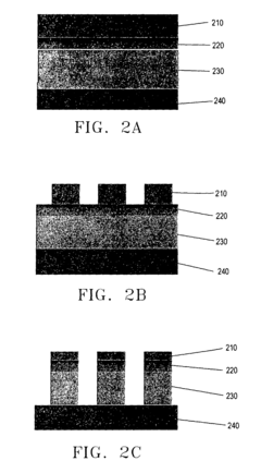
- Specialized CVD techniques and modifications: Specialized Chemical Vapor Deposition techniques and modifications include Plasma-Enhanced CVD (PECVD), Atomic Layer Deposition (ALD), Metal-Organic CVD (MOCVD), and other variants that address specific deposition challenges. These techniques modify the conventional CVD process by introducing additional energy sources, pulsed precursor delivery, or other enhancements to achieve improved film properties, lower deposition temperatures, better step coverage, or higher purity films. Such specialized approaches extend the capabilities of CVD for advanced materials and applications.
02 Precursor delivery and gas flow control in CVD processes
Methods and systems for precise delivery of precursor materials and control of gas flow in Chemical Vapor Deposition processes. These innovations focus on optimizing precursor vaporization, transport mechanisms, flow rate control, and mixing techniques to achieve consistent film deposition. Advanced gas delivery systems enable better control over reaction kinetics and film properties during the deposition process.Expand Specific Solutions03 CVD for semiconductor device fabrication
Applications of Chemical Vapor Deposition specifically for semiconductor manufacturing, including deposition of dielectric layers, conductive films, and barrier materials. These techniques are optimized for microelectronic device fabrication with focus on conformality, step coverage, and integration with other semiconductor processing steps. The methods address challenges in advanced node technologies including high aspect ratio structures and complex device architectures.Expand Specific Solutions04 Plasma-enhanced and modified CVD techniques
Enhanced Chemical Vapor Deposition methods that utilize plasma or other energy sources to modify the deposition process. These techniques include plasma-enhanced CVD (PECVD), remote plasma CVD, and other modified approaches that use additional energy to activate precursors, lower deposition temperatures, or improve film properties. The plasma enhancement allows for deposition at lower temperatures while maintaining or improving film quality and deposition rates.Expand Specific Solutions05 Novel materials and thin films by CVD
Development of processes for depositing novel materials and specialized thin films using Chemical Vapor Deposition. These include methods for depositing advanced materials such as high-k dielectrics, low-k materials, metal films, compound semiconductors, and functional coatings. The processes are tailored to achieve specific material properties, compositions, and structures for various applications including electronics, optics, and protective coatings.Expand Specific Solutions
Key Industry Players and Competitive Landscape
The plasma-enhanced chemical vapor deposition (PECVD) versus thermal CVD market is currently in a growth phase, with major semiconductor equipment manufacturers like Applied Materials, Tokyo Electron, and Samsung Electronics dominating the competitive landscape. The global CVD market is projected to reach approximately $35 billion by 2027, driven by increasing demand for advanced semiconductor devices and display technologies. PECVD technology has gained significant traction due to its lower processing temperatures and enhanced film properties, with companies like Oxford Instruments and Centrotherm developing specialized solutions. Established players are focusing on integration capabilities and comprehensive process solutions, while emerging companies like LeydenJar Technologies are targeting niche applications such as battery technology. The competitive dynamics are characterized by continuous innovation in precursor chemistry, plasma source design, and process control systems.
Applied Materials, Inc.
Technical Solution: Applied Materials has developed advanced plasma-enhanced chemical vapor deposition (PECVD) systems that operate at lower temperatures (200-400°C) compared to thermal CVD (>800°C). Their Producer® platform incorporates multi-station sequential deposition technology with independent plasma sources for each chamber, enabling precise control over film properties. The company's PECVD technology utilizes radio frequency (RF) power to create reactive plasma that allows deposition of high-quality silicon nitride, silicon oxide, and amorphous silicon films at significantly lower temperatures than thermal processes. Their dual-frequency PECVD capability enables independent control of ion energy and plasma density, resulting in films with tailored stress characteristics and improved step coverage[1]. Applied Materials has also pioneered high-density plasma CVD (HDP-CVD) systems that combine physical sputtering with chemical deposition for superior gap-filling performance in high-aspect-ratio structures, critical for advanced semiconductor manufacturing nodes[3].
Strengths: Lower thermal budget allowing for temperature-sensitive substrate compatibility; better step coverage for complex topographies; ability to deposit films with controlled stress; higher throughput due to faster deposition rates. Weaknesses: More complex equipment design leading to higher maintenance requirements; potential for plasma-induced damage to underlying layers; higher capital equipment costs compared to thermal CVD systems.
Tokyo Electron Ltd.
Technical Solution: Tokyo Electron (TEL) has developed the TRIAS™ SPA (Spatial Plasma Atomic Layer) system that combines PECVD technology with atomic layer deposition principles. This hybrid approach enables ultra-thin film deposition with atomic-level precision while maintaining high throughput. Their PECVD technology employs a unique spatial separation of precursor and plasma activation zones, reducing plasma damage while enhancing film quality. TEL's thermal CVD portfolio includes the TELFORMULA™ system, which utilizes hot-wall reactor design for optimal thermal efficiency and process uniformity across 300mm wafers. The company has pioneered advanced precursor delivery systems for both technologies, with their thermal CVD focusing on high-temperature (600-900°C) processes for polysilicon, silicon nitride, and high-k dielectric materials[2]. TEL's comparative studies have demonstrated that their PECVD processes achieve 30-40% lower hydrogen content in silicon nitride films compared to thermal CVD, resulting in improved electrical properties and reduced post-deposition annealing requirements[4].
Strengths: Specialized equipment for both PECVD and thermal CVD allowing process optimization based on application requirements; advanced precursor delivery systems improving film uniformity; industry-leading process control software integration. Weaknesses: Higher equipment complexity requiring specialized maintenance expertise; thermal CVD systems have lower throughput for certain applications compared to PECVD alternatives; higher energy consumption for thermal processes.
Critical Patents and Research Breakthroughs
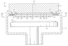
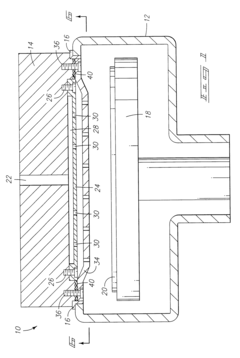
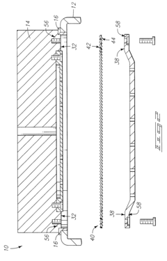
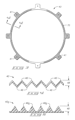
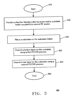
Plasma enhanced chemical vapor deposition process
PatentInactiveUS6468925B2
Innovation
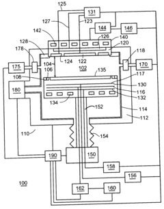
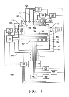
- A preformed electrically conductive gasket is interposed between the RF powered showerhead support electrode and the gas distributing showerhead, facilitating consistent RF electrical contact by accommodating thermal expansion differences and maintaining a stable connection during assembly and disassembly.
Method and apparatus for depositing materials with tunable optical properties and etching characteristics
PatentInactiveUS20050039681A1
Innovation
- A plasma-enhanced chemical vapor deposition (PECVD) system is used to deposit a Tunable Etch Resistant ARC (TERA) layer, where the physical, chemical, or optical properties of the layer are dependent on the amount of RF power provided, and the deposition rate is controlled by varying the RF power, allowing for precise tuning of the film properties.
Environmental Impact and Sustainability Considerations
The environmental impact of chemical vapor deposition (CVD) processes has become increasingly important as industries strive for more sustainable manufacturing practices. When comparing Plasma Enhanced Chemical Vapor Deposition (PECVD) and Thermal CVD, several key environmental considerations emerge that significantly influence their adoption in various applications.
PECVD generally operates at lower temperatures (200-400°C) compared to Thermal CVD (600-1000°C), resulting in substantially reduced energy consumption. This temperature difference translates to approximately 30-50% energy savings in industrial applications, making PECVD a more energy-efficient option in many scenarios. The reduced energy footprint directly correlates with lower carbon emissions, particularly important in regions where electricity generation relies heavily on fossil fuels.
Precursor utilization efficiency represents another critical environmental factor. PECVD typically achieves 40-60% precursor utilization rates compared to Thermal CVD's 20-40%, due to the plasma's ability to more effectively activate reactant species. This higher efficiency reduces chemical waste and decreases the environmental burden associated with precursor production and disposal.
Both processes utilize potentially hazardous gases such as silane (SiH₄), phosphine (PH₃), and various fluorinated compounds. However, PECVD systems often incorporate more advanced abatement systems due to their more recent technological development. Modern PECVD facilities typically feature point-of-use abatement with destruction removal efficiencies exceeding 99% for most harmful byproducts.
Water consumption patterns differ significantly between these technologies. Thermal CVD systems generally require more extensive cooling systems due to their higher operating temperatures, resulting in greater water usage. PECVD systems typically consume 20-30% less cooling water, an increasingly important consideration in water-stressed regions.
The lifecycle assessment of equipment reveals that PECVD systems generally have shorter operational lifespans (7-10 years) compared to Thermal CVD equipment (10-15 years), potentially increasing electronic waste. However, newer PECVD systems incorporate more recyclable components and modular designs that facilitate parts replacement rather than complete system disposal.
Regulatory compliance represents an evolving challenge for both technologies. Recent environmental regulations in Europe, North America, and parts of Asia have imposed stricter limits on perfluorinated compounds and other greenhouse gases commonly used in CVD processes. PECVD processes can more readily adapt to alternative, environmentally benign precursors due to their lower temperature requirements and plasma activation capabilities.
Cost-Benefit Analysis of Implementation Strategies
When evaluating implementation strategies for Chemical Vapor Deposition (CVD) technologies, a comprehensive cost-benefit analysis reveals significant differences between Plasma Enhanced CVD (PECVD) and Thermal CVD approaches. The initial capital investment for PECVD systems typically exceeds that of thermal CVD by 30-45%, primarily due to the additional plasma generation equipment, RF power supplies, and more complex vacuum systems required. However, this higher upfront cost must be weighed against operational advantages.
Energy consumption patterns differ substantially between these technologies. Thermal CVD processes operate at temperatures ranging from 600°C to over 1000°C, resulting in significant energy costs for heating and maintaining these elevated temperatures. In contrast, PECVD systems operate at lower temperatures (200-400°C) but require additional energy for plasma generation. Studies indicate that PECVD can achieve 15-25% energy savings in long-term operations, particularly for temperature-sensitive applications.
Maintenance requirements and system longevity also factor prominently in implementation decisions. PECVD systems contain more complex components subject to wear, particularly plasma electrodes and RF matching networks, resulting in approximately 20% higher annual maintenance costs. However, thermal CVD systems often experience more severe thermal cycling effects, potentially reducing overall equipment lifespan.
Production efficiency metrics favor PECVD in many applications. The lower processing temperatures enable faster heating and cooling cycles, reducing batch processing times by up to 40% compared to thermal CVD. This throughput advantage can significantly offset the higher initial investment, particularly in high-volume manufacturing environments.
Material compatibility considerations also impact implementation economics. PECVD's lower temperature operation expands the range of viable substrate materials, potentially reducing material costs by 10-30% through the use of less expensive temperature-sensitive substrates. This advantage becomes particularly significant in applications like flexible electronics and certain semiconductor packaging processes.
Quality-related costs must be factored into implementation strategies as well. PECVD typically produces films with fewer thermal stress-induced defects, potentially improving yield rates by 5-15% compared to thermal processes. This quality advantage translates directly to reduced scrap rates and rework costs in production environments.
Return on investment (ROI) calculations indicate that despite higher initial costs, PECVD implementation strategies typically achieve breakeven points within 2-3 years in high-volume applications, while thermal CVD may be more economically viable for lower-volume, less temperature-sensitive processes where initial capital conservation is prioritized over operational efficiency.
Unlock deeper insights with Patsnap Eureka Quick Research — get a full tech report to explore trends and direct your research. Try now!
Generate Your Research Report Instantly with AI Agent
Supercharge your innovation with Patsnap Eureka AI Agent Platform!