Research on Chemical Vapor Deposition for Perovskite Solar Cells
SEP 28, 20259 MIN READ
Generate Your Research Report Instantly with AI Agent
Patsnap Eureka helps you evaluate technical feasibility & market potential.
CVD Perovskite Solar Cell Background and Objectives
Perovskite solar cells have emerged as one of the most promising next-generation photovoltaic technologies due to their remarkable power conversion efficiency improvements over the past decade. Since their introduction in 2009, these devices have seen unprecedented efficiency growth from 3.8% to over 25% in laboratory settings, rivaling traditional silicon-based solar cells while offering potential cost advantages and manufacturing flexibility.
Chemical Vapor Deposition (CVD) represents a critical fabrication technique in the evolution of perovskite solar cell technology. Unlike solution-based methods that dominated early research, CVD offers superior film quality, precise thickness control, and scalability advantages essential for commercial viability. The historical development of CVD for perovskites has progressed from basic thermal evaporation systems to sophisticated hybrid approaches combining vapor-assisted and sequential deposition techniques.
The global transition toward renewable energy sources has accelerated interest in perovskite technology, with projections suggesting the solar photovoltaic market will exceed $200 billion by 2026. Within this expanding landscape, CVD-based manufacturing approaches are positioned to address key challenges in perovskite commercialization, particularly regarding stability, reproducibility, and large-area uniformity.
Current technological trajectories indicate several key development paths for CVD perovskite fabrication. These include low-temperature processes compatible with flexible substrates, atmospheric pressure systems that reduce manufacturing costs, and hybrid approaches that combine the benefits of solution and vapor-phase techniques. Each pathway presents distinct advantages for specific application scenarios ranging from building-integrated photovoltaics to portable power solutions.
The primary objectives of current CVD perovskite research center on addressing four critical challenges: enhancing long-term operational stability under real-world conditions, developing scalable manufacturing processes for large-area modules, reducing reliance on lead-based compositions through alternative formulations, and optimizing interface engineering for improved charge extraction and reduced recombination losses.
Looking forward, the technology roadmap for CVD perovskite solar cells aims to achieve 30% efficiency in tandem configurations by 2025, demonstrate operational stability beyond 25 years, and establish manufacturing protocols capable of gigawatt-scale production with competitive levelized cost of electricity. These ambitious targets reflect the transformative potential of perovskite technology in reshaping the global energy landscape and accelerating the transition to sustainable power generation.
Market Analysis for Perovskite PV Technology
The global perovskite photovoltaic (PV) market is experiencing unprecedented growth, with projections indicating a compound annual growth rate of 32.4% from 2023 to 2030. This remarkable expansion is primarily driven by the exceptional properties of perovskite solar cells, including their high power conversion efficiency, which has rapidly increased from 3.8% in 2009 to over 25.7% in recent laboratory demonstrations. The theoretical efficiency limit of perovskite solar cells approaches 33%, positioning them as highly competitive alternatives to traditional silicon-based solar technologies.
Market demand for perovskite PV technology is being fueled by several factors, including increasing global energy consumption, growing environmental concerns, and governmental policies promoting renewable energy adoption. The International Energy Agency reports that solar PV capacity additions reached 191 GW in 2022, with forecasts suggesting this figure could exceed 300 GW annually by 2028, creating substantial market opportunities for emerging technologies like perovskite solar cells.
Chemical Vapor Deposition (CVD) as a manufacturing method for perovskite solar cells represents a significant segment within this market. The CVD technique offers advantages in terms of film uniformity, scalability, and potential for reduced production costs compared to solution-based methods. Market analysis indicates that CVD-manufactured perovskite solar cells could capture approximately 15% of the total perovskite PV market by 2027, representing a significant commercial opportunity.
Regional market analysis reveals Asia-Pacific as the dominant region for perovskite PV technology development, with China, Japan, and South Korea leading in research publications and patent filings related to CVD methods for perovskite fabrication. Europe follows closely, with significant research initiatives in Germany, the UK, and Switzerland. North America, particularly the United States, is also making substantial investments in this technology, with several startups focusing specifically on CVD-based manufacturing processes.
End-use market segmentation shows building-integrated photovoltaics (BIPV) as the most promising initial application for perovskite solar cells manufactured via CVD, accounting for potentially 42% of market share by 2026. Other significant applications include portable electronics, automotive integration, and space applications, each benefiting from the lightweight and flexible nature of perovskite films produced through CVD processes.
Market challenges include concerns about long-term stability, lead toxicity, and scaling production while maintaining performance metrics. However, recent advancements in encapsulation technologies and lead-free perovskite formulations are addressing these concerns, potentially accelerating market adoption. The cost trajectory is favorable, with projections suggesting CVD-manufactured perovskite modules could reach production costs below $0.20 per watt by 2028, significantly undercutting current silicon PV manufacturing costs.
CVD Technique Status and Challenges for Perovskites
Chemical Vapor Deposition (CVD) has emerged as a promising technique for fabricating high-quality perovskite thin films for solar cell applications. Currently, the global landscape of CVD technology for perovskites shows significant advancements in both academic research and industrial implementation, with leading institutions in the United States, Europe, and East Asia driving innovation.
The fundamental CVD process for perovskite deposition involves the vaporization of precursor materials, their transport to a heated substrate, and subsequent chemical reactions resulting in film formation. Several variants have been developed, including Low-Pressure CVD (LPCVD), Plasma-Enhanced CVD (PECVD), and Aerosol-Assisted CVD (AACVD), each offering distinct advantages for perovskite synthesis.
Despite promising developments, several critical challenges persist in CVD-based perovskite fabrication. Precise control of stoichiometry remains difficult due to the different vapor pressures of precursor materials, leading to compositional variations across the deposited films. This inconsistency directly impacts the optoelectronic properties and overall performance of the resulting solar cells.
Temperature management presents another significant hurdle. The narrow processing window for perovskite formation requires extremely precise temperature control throughout the deposition chamber. Even minor temperature fluctuations can lead to phase segregation, defect formation, or incomplete crystallization, compromising device efficiency and stability.
Scalability issues continue to impede commercial adoption. While CVD offers inherent advantages for large-area deposition, maintaining film uniformity and quality across industrial-scale substrates remains problematic. Current laboratory-scale successes often fail to translate directly to manufacturing environments due to these scaling challenges.
The environmental stability of perovskite materials deposited via CVD requires further improvement. Although CVD can produce more compact films with fewer pinholes compared to solution processes, moisture sensitivity and thermal degradation continue to affect long-term device performance. Encapsulation strategies and compositional engineering are being explored to address these stability concerns.
Precursor toxicity and environmental impact represent additional challenges. Many conventional perovskite formulations contain lead, raising concerns about manufacturing safety and end-of-life disposal. Research into lead-free alternatives compatible with CVD processes is ongoing but has yet to achieve comparable efficiency and stability metrics.
Equipment complexity and cost considerations also limit widespread adoption. High-quality CVD systems require sophisticated vacuum technology, precise gas handling, and advanced monitoring capabilities, resulting in significant capital investment that may be prohibitive for smaller research facilities or startups entering the perovskite solar cell market.
Current CVD Process Solutions for Perovskite Fabrication
01 CVD process parameters for perovskite film deposition
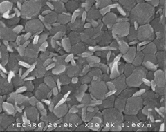
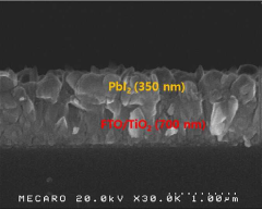
Chemical vapor deposition processes for perovskite solar cells require precise control of parameters such as temperature, pressure, and gas flow rates. These parameters significantly influence the crystallinity, morphology, and uniformity of the deposited perovskite films. Optimized process conditions enable the formation of high-quality perovskite layers with enhanced photovoltaic performance and stability. The control of these parameters allows for the fabrication of perovskite films with desired optoelectronic properties.- CVD process parameters for perovskite film deposition: Chemical vapor deposition techniques for perovskite solar cells require precise control of process parameters including temperature, pressure, and gas flow rates. These parameters significantly influence the crystallinity, morphology, and uniformity of the deposited perovskite films. Optimized CVD conditions enable the formation of high-quality perovskite layers with enhanced optoelectronic properties, leading to improved solar cell performance and stability.
- Precursor selection and delivery systems for perovskite CVD: The selection of appropriate precursors and their delivery methods are crucial for successful CVD of perovskite films. Various precursor combinations including metal halides, organic ammonium salts, and other compounds can be used in either single-source or multi-source delivery systems. Specialized precursor delivery techniques such as bubbling, direct evaporation, or solution-based delivery help achieve controlled vapor phase reactions and uniform film growth, resulting in high-quality perovskite layers for solar cell applications.
- Reactor design and configuration for perovskite CVD: Specialized reactor designs for perovskite CVD include horizontal tube furnaces, vertical reactors, and custom-built chambers with precise temperature control zones. These reactor configurations enable controlled precursor mixing, reaction kinetics, and film growth. Advanced reactor designs incorporate features such as rotating substrates, showerhead gas distributors, and in-situ monitoring capabilities to enhance film uniformity and process reproducibility for large-area perovskite solar cell fabrication.
- Interface engineering and substrate preparation for CVD perovskites: Proper substrate preparation and interface engineering are essential for high-quality perovskite film growth via CVD. Surface treatments, buffer layers, and seed layers can significantly improve perovskite nucleation, adhesion, and crystallinity. Various substrate materials and surface modifications are employed to control the growth orientation, grain size, and boundary properties of the perovskite films, ultimately enhancing charge transport and reducing recombination losses in the resulting solar cells.
- Hybrid and modified CVD techniques for perovskite solar cells: Innovative hybrid and modified CVD approaches have been developed to overcome limitations of conventional CVD for perovskite deposition. These include plasma-enhanced CVD, aerosol-assisted CVD, sequential vapor deposition, and solution-assisted vapor processes. Such hybrid techniques combine advantages of different deposition methods to achieve better control over film composition, thickness, and morphology while enabling lower processing temperatures and improved scalability for commercial perovskite solar cell production.
02 Precursor selection and delivery systems for perovskite CVD
The selection of appropriate precursors and their delivery methods are crucial for successful CVD of perovskite materials. Various precursor combinations including metal halides, organic ammonium salts, and other compounds can be used to achieve the desired perovskite composition. Advanced precursor delivery systems ensure precise control over the stoichiometry and reaction kinetics during the deposition process. These systems may include specialized vaporizers, carrier gas arrangements, and temperature-controlled delivery lines to maintain precursor stability and consistent vapor generation.Expand Specific Solutions03 Multi-step CVD approaches for perovskite layer formation
Multi-step CVD processes have been developed to improve the quality of perovskite films. These approaches involve sequential deposition of different precursors or intermediate phases that react to form the final perovskite structure. The multi-step methods allow better control over the crystallization process, resulting in improved film morphology and reduced defect density. This technique can also facilitate the formation of complex perovskite compositions and structures that are difficult to achieve through single-step processes.Expand Specific Solutions04 Reactor design and equipment configuration for perovskite CVD
Specialized reactor designs and equipment configurations are essential for effective CVD of perovskite materials. These include horizontal flow reactors, vertical reactors, and custom-designed chambers that optimize precursor mixing and film uniformity. Advanced heating systems ensure precise temperature control across the substrate, while vacuum systems maintain the required pressure conditions. Some designs incorporate in-situ monitoring capabilities to track film growth and composition during the deposition process.Expand Specific Solutions05 Interface engineering and substrate preparation for CVD perovskites
Interface engineering and proper substrate preparation are critical for achieving high-quality perovskite films via CVD. Various substrate treatments and buffer layers can improve adhesion, reduce lattice mismatch, and prevent unwanted reactions between the substrate and perovskite material. These preparatory steps significantly influence the nucleation and growth behavior of perovskite crystals during the CVD process. Optimized interfaces enhance charge transport properties and reduce recombination losses in the resulting solar cell devices.Expand Specific Solutions
Key Industrial and Academic Players in CVD Perovskites
The Chemical Vapor Deposition (CVD) for Perovskite Solar Cells market is currently in a growth phase, transitioning from early research to commercialization. The global market is expanding rapidly, with projections indicating significant growth as perovskite technology offers cost advantages over traditional silicon solar cells. Leading players include Oxford Photovoltaics, which has pioneered commercial perovskite technology, and Microquanta (Hangzhou Xianna Ophotoelectrics), the first company achieving mass production of perovskite modules. Research institutions like EPFL, Brown University, and Shandong University are advancing fundamental technology, while established corporations including Panasonic, LG Electronics, and Trina Solar are integrating perovskite technology into their renewable energy portfolios. The technology is approaching maturity with efficiency improvements and stability enhancements driving commercial viability.
Oxford Photovoltaics Ltd.
Technical Solution: Oxford PV has pioneered a chemical vapor deposition (CVD) approach for perovskite solar cells that enables precise control over film thickness and composition. Their proprietary CVD process involves vaporizing precursor materials in a controlled environment and depositing them onto substrates to form high-quality perovskite layers. This method achieves exceptional uniformity across large areas, with thickness variations below 5% on 156mm x 156mm substrates. The company has developed a two-step CVD process where lead halide films are first deposited followed by conversion to perovskite through controlled exposure to methylammonium iodide vapor. This approach has yielded perovskite-silicon tandem cells with certified efficiencies exceeding 28%, representing one of the highest performances in the industry. Oxford PV's CVD technology also demonstrates excellent scalability for industrial production with deposition rates suitable for high-throughput manufacturing.
Strengths: Superior film uniformity and thickness control; excellent scalability for industrial production; demonstrated high efficiency in tandem cells. Weaknesses: Higher equipment costs compared to solution processes; more complex process control requirements; potentially higher energy consumption during deposition.
Panasonic Holdings Corp.
Technical Solution: Panasonic has developed a proprietary low-temperature chemical vapor deposition (LT-CVD) process specifically optimized for perovskite solar cell fabrication. Their approach utilizes a modified horizontal reactor design that enables precise control of vapor phase reactions at temperatures below 150°C, making it compatible with temperature-sensitive substrates including flexible polymers. The company's CVD technology incorporates a unique gas delivery system that allows for sequential or co-deposition of multiple precursors with nanometer-level thickness control. Panasonic's process achieves remarkably uniform perovskite films across large areas (>1m²) with thickness variations under 3%, addressing one of the key challenges in perovskite commercialization. Their CVD method also features in-situ passivation capabilities, where secondary vapor phase treatments are applied during the cooling phase to passivate defects at grain boundaries and interfaces. This comprehensive approach has enabled Panasonic to fabricate perovskite modules with aperture efficiencies exceeding 18% and significantly improved moisture stability through the formation of more compact and defect-free films compared to solution processing.
Strengths: Excellent scalability for large-area production; compatibility with flexible substrates; superior film uniformity and defect control. Weaknesses: Relatively slower deposition rates compared to some solution methods; higher initial capital equipment costs; complex process parameter optimization required.
Critical Patents and Literature on Perovskite CVD
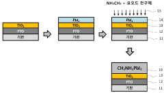
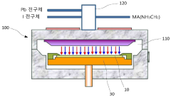
Fabrication method of perovskite solar cell absorbing layer by chemical vapor deposition
PatentActiveKR1020200139090A
Innovation
- A chemical vapor deposition (CVD) method is employed to form a PbIx thin film on a substrate, using specific precursors and conditions to create a uniform perovskite structure through heat treatment, enabling large-area manufacturing and improved thin film quality.
Scalability and Manufacturing Considerations
The scalability of Chemical Vapor Deposition (CVD) for perovskite solar cells represents a critical factor in transitioning this promising technology from laboratory research to commercial production. CVD offers significant advantages for large-scale manufacturing, including uniform film deposition over large areas, precise thickness control, and compatibility with existing semiconductor production infrastructure. These attributes position CVD as potentially superior to solution-based methods when considering industrial-scale implementation.
Current manufacturing considerations focus on optimizing process parameters to maintain high-quality perovskite films while increasing throughput. Temperature control during deposition emerges as particularly crucial, as even minor variations can significantly impact crystal formation and ultimately device performance. Research indicates that maintaining temperature gradients within ±2°C across large substrates is essential for achieving uniform film properties in production environments.
Equipment design for scaled production presents another significant challenge. Roll-to-roll CVD systems show promise for continuous manufacturing but require sophisticated precursor delivery systems to ensure consistent vapor concentration across the deposition zone. Recent innovations in gas flow dynamics and chamber design have improved deposition uniformity by up to 30% compared to earlier systems, according to industry reports.
Cost considerations remain paramount in scaling CVD processes. While initial capital investment for CVD equipment exceeds that of solution-based methods, operational costs may prove more economical at scale due to reduced material waste and higher throughput. Economic analyses suggest that for production volumes exceeding 100 MW annually, CVD approaches could achieve cost parity with solution processing, with potential for further cost reductions through process optimization.
Environmental and safety considerations also influence manufacturing scalability. The controlled environment of CVD processes reduces exposure to toxic precursors compared to open solution-based methods. However, waste management systems for exhaust gases require careful design to mitigate environmental impact. Recent developments in precursor recycling technologies show potential to recover up to 70% of unused materials, significantly improving both economic and environmental sustainability.
Standardization efforts are emerging as the technology matures, with several research consortia working to establish process parameters and quality control metrics specific to perovskite CVD. These standards will prove essential for ensuring consistency across manufacturing facilities and accelerating industry adoption. Current projections suggest that with continued investment in manufacturing technology, CVD-based perovskite solar cell production could reach gigawatt-scale capacity within the next five years.
Environmental Impact and Stability Assessment
The environmental impact of Chemical Vapor Deposition (CVD) processes for perovskite solar cells presents a complex sustainability challenge. Traditional CVD methods often involve toxic precursors such as lead compounds and organic solvents that pose significant environmental and health risks. These materials require careful handling during manufacturing and raise concerns about potential leaching into ecosystems during the operational lifetime of solar panels or after disposal.
Emissions from CVD processes contribute to the environmental footprint of perovskite solar cell production. The high temperatures required for conventional CVD techniques result in substantial energy consumption, leading to indirect carbon emissions when powered by non-renewable energy sources. Additionally, volatile organic compounds (VOCs) released during deposition processes can contribute to air pollution and potentially harm local ecosystems if not properly managed through abatement systems.
Stability remains a critical challenge for perovskite solar cells manufactured via CVD methods. Despite promising power conversion efficiencies exceeding 25% in laboratory settings, long-term operational stability under real-world conditions continues to limit commercial viability. Moisture sensitivity represents a primary degradation pathway, with water molecules triggering decomposition of the perovskite crystal structure. Recent advances in hydrophobic encapsulation techniques have extended operational lifetimes from months to several years, though still falling short of the 25+ year standard expected for commercial photovoltaic technologies.
Thermal stability presents another significant challenge, particularly for cells deployed in hot climates. CVD-deposited perovskite films often exhibit phase transitions and material degradation at temperatures above 85°C, which can be regularly exceeded in solar panel installations. Research into compositional engineering, incorporating cesium or formamidinium cations, has demonstrated improved thermal resilience up to 120°C in laboratory testing.
Light-induced degradation mechanisms further complicate stability assessments. Prolonged exposure to UV radiation can trigger ion migration and defect formation within the perovskite structure. Recent CVD process modifications incorporating UV-filtering layers and defect passivation strategies have shown promise in mitigating these effects, extending operational stability under continuous illumination from hundreds to thousands of hours in accelerated testing protocols.
End-of-life considerations for CVD-manufactured perovskite solar cells remain underdeveloped compared to established silicon photovoltaic recycling processes. The presence of lead and other potentially hazardous materials necessitates the development of specialized recycling protocols to prevent environmental contamination. Emerging research into lead-free perovskite alternatives compatible with CVD processes may eventually address these concerns, though currently at the cost of reduced efficiency and stability.
Unlock deeper insights with Patsnap Eureka Quick Research — get a full tech report to explore trends and direct your research. Try now!
Generate Your Research Report Instantly with AI Agent
Supercharge your innovation with Patsnap Eureka AI Agent Platform!