Comparative Study of Chemical Vapor Deposition vs Atomic Layer Deposition
SEP 28, 20259 MIN READ
Generate Your Research Report Instantly with AI Agent
Patsnap Eureka helps you evaluate technical feasibility & market potential.
CVD and ALD Technology Background and Objectives
Chemical Vapor Deposition (CVD) and Atomic Layer Deposition (ALD) represent two cornerstone technologies in thin film deposition processes that have revolutionized semiconductor manufacturing, microelectronics, and various advanced material applications. CVD, with its origins dating back to the late 19th century, gained significant industrial traction in the 1960s with the rise of integrated circuit manufacturing. The technology evolved from basic thermal CVD to more sophisticated variants including plasma-enhanced CVD (PECVD), metal-organic CVD (MOCVD), and low-pressure CVD (LPCVD), each addressing specific application requirements.
ALD emerged later as a specialized offshoot of CVD, with its fundamental principles established in the 1970s by Finnish scientist Tuomo Suntola. Initially termed "atomic layer epitaxy," ALD gained prominence in the early 2000s as semiconductor feature sizes shrank below 100 nanometers, necessitating atomic-level precision in deposition processes. The technology's self-limiting reaction mechanism represented a paradigm shift in thin film deposition methodology.
The evolution trajectory of both technologies has been driven by the relentless miniaturization in microelectronics, following Moore's Law, and the increasing demand for high-performance materials with precisely controlled properties. While CVD has maintained its position as a versatile, high-throughput deposition method, ALD has carved its niche in applications requiring exceptional conformality and thickness control at the atomic scale.
Current industry trends indicate a growing convergence between these technologies, with hybrid approaches emerging to leverage the advantages of both. The development of spatial ALD and high-throughput CVD variants demonstrates the industry's push toward balancing precision with productivity. Additionally, both technologies are expanding beyond traditional semiconductor applications into emerging fields such as energy storage, photovoltaics, and biomedical devices.
The primary technical objective of this comparative study is to establish a comprehensive understanding of the fundamental principles, capabilities, limitations, and application domains of CVD and ALD. This includes analyzing the process parameters, reaction mechanisms, equipment requirements, and economic considerations that influence technology selection for specific applications.
Furthermore, this study aims to identify potential innovation pathways that could address current limitations in both technologies, particularly focusing on throughput challenges in ALD and precision control in CVD. By mapping the technological landscape and evolutionary trajectory, we seek to provide strategic insights for research prioritization and technology investment decisions in advanced manufacturing contexts.
Market Demand Analysis for Thin Film Deposition Technologies
The global thin film deposition technology market has experienced significant growth in recent years, driven primarily by the semiconductor industry's continuous pursuit of miniaturization and enhanced performance. Current market valuations place the thin film deposition sector at approximately 22 billion USD in 2023, with projections indicating a compound annual growth rate (CAGR) of 8.5% through 2030, potentially reaching 39 billion USD by the end of the decade.
Chemical Vapor Deposition (CVD) and Atomic Layer Deposition (ALD) represent two critical segments within this market, with distinct demand profiles. CVD currently holds the larger market share at roughly 60% of thin film applications, particularly dominating in traditional semiconductor manufacturing, solar panels, and protective coatings. However, ALD is experiencing more rapid growth, with a CAGR exceeding 12%, outpacing the broader market.
This accelerated demand for ALD technology stems from the semiconductor industry's transition to sub-5nm process nodes, where atomic-level precision becomes non-negotiable. Major semiconductor manufacturers have increased their capital expenditure on ALD equipment by approximately 15% year-over-year since 2020, reflecting the critical role this technology plays in advanced node development.
Regional analysis reveals Asia-Pacific as the dominant market for both technologies, accounting for over 65% of global demand. This concentration aligns with the region's semiconductor manufacturing footprint, particularly in Taiwan, South Korea, and increasingly, mainland China. North America and Europe follow with approximately 20% and 12% market share respectively, with particular emphasis on specialized applications in aerospace, medical devices, and emerging quantum computing hardware.
End-user segmentation shows semiconductors and electronics consuming nearly 70% of thin film deposition capacity, followed by solar energy applications at 15%, and various industrial applications comprising the remainder. Within the semiconductor segment, logic and memory manufacturers represent the largest customer base, though emerging applications in MEMS, sensors, and advanced packaging are growing at above-market rates.
Customer requirements are increasingly diverging between CVD and ALD applications. CVD users prioritize throughput and cost-effectiveness for relatively thicker films, while ALD customers emphasize precision, uniformity, and the ability to deposit ultra-thin conformal layers on complex 3D structures. This bifurcation in market demands is driving equipment manufacturers to develop specialized solutions rather than one-size-fits-all approaches.
Market forecasts indicate continued strong growth for both technologies, with ALD expected to gradually increase its market share as device architectures become more complex and three-dimensional. The emergence of new materials requiring precise atomic-level deposition, particularly for next-generation memory and quantum computing applications, will further accelerate ALD adoption in specialized high-value segments.
Current State and Technical Challenges in CVD vs ALD
Chemical Vapor Deposition (CVD) and Atomic Layer Deposition (ALD) represent two cornerstone technologies in thin film deposition, with global market valuations reaching approximately $23 billion and $2.5 billion respectively in 2022. CVD technology has matured significantly since its industrial adoption in the 1960s, while ALD has experienced accelerated development since the early 2000s, particularly in semiconductor manufacturing.
Currently, CVD processes dominate in applications requiring thicker films (>100nm) and higher deposition rates, such as in solar panel manufacturing, protective coatings, and certain semiconductor processes. The technology excels in cost-effectiveness for large-area applications but faces challenges in achieving precise thickness control below 10nm and uniform step coverage on complex 3D structures with high aspect ratios.
ALD, conversely, has established itself as the premier solution for ultra-thin film deposition with atomic-level precision. Its self-limiting reaction mechanism enables unparalleled conformality on complex geometries and precise thickness control at the angstrom level. However, ALD processes typically operate at deposition rates 10-100 times slower than CVD, presenting significant throughput limitations for industrial-scale production.
The geographical distribution of these technologies shows interesting patterns. While North America and Europe lead in ALD research and innovation, East Asian countries—particularly South Korea, Japan, and Taiwan—dominate in industrial implementation, especially in semiconductor manufacturing. China has rapidly expanded its capabilities in both technologies over the past decade, particularly in solar applications.
Technical challenges for CVD include reducing process temperatures to enable compatibility with temperature-sensitive substrates, minimizing precursor waste, and improving film quality at higher deposition rates. Environmental concerns regarding precursor toxicity and energy consumption also present significant hurdles for wider adoption.
For ALD, the primary challenges revolve around throughput limitations, precursor development for new materials, and scaling processes for larger substrates. The industry is actively pursuing spatial ALD and multi-wafer batch processing to address throughput issues, while research into novel precursors aims to expand the material palette beyond oxides and nitrides.
Both technologies face integration challenges with emerging device architectures, particularly as feature sizes continue to shrink below 3nm in advanced semiconductor nodes. The development of hybrid approaches combining CVD and ALD processes represents a promising direction to leverage the advantages of both technologies while mitigating their respective limitations.
Current Technical Solutions in CVD and ALD Applications
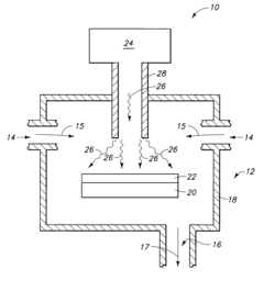
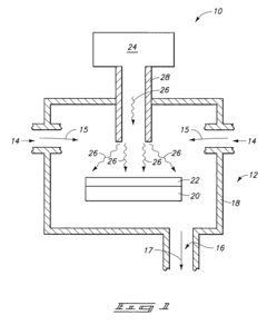
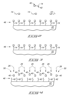
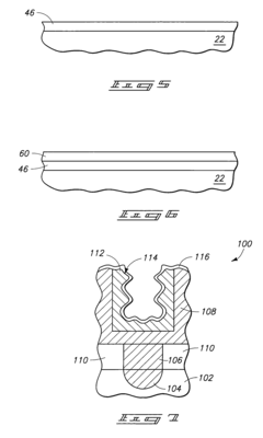
01 Fundamental principles and processes of CVD and ALD
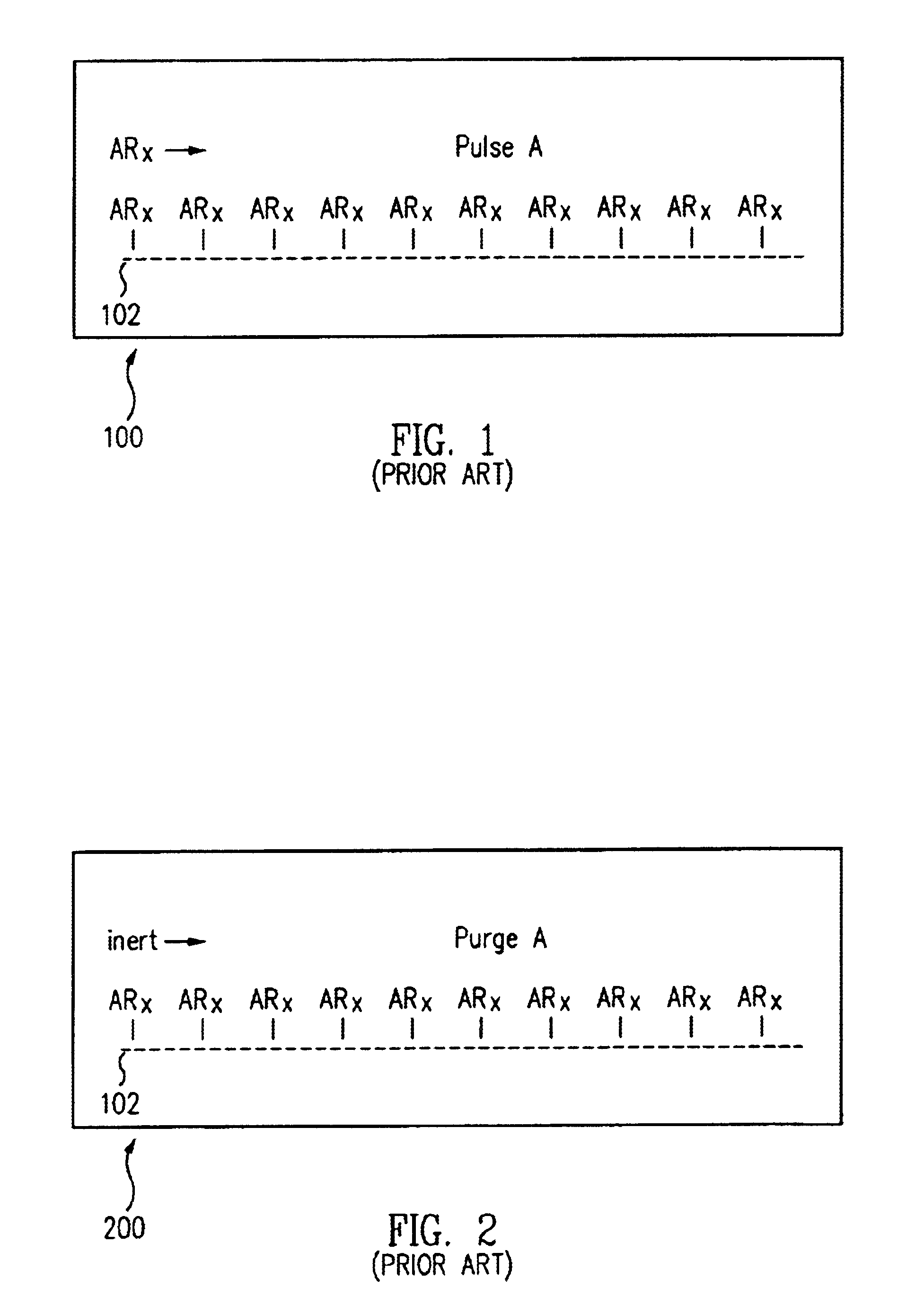
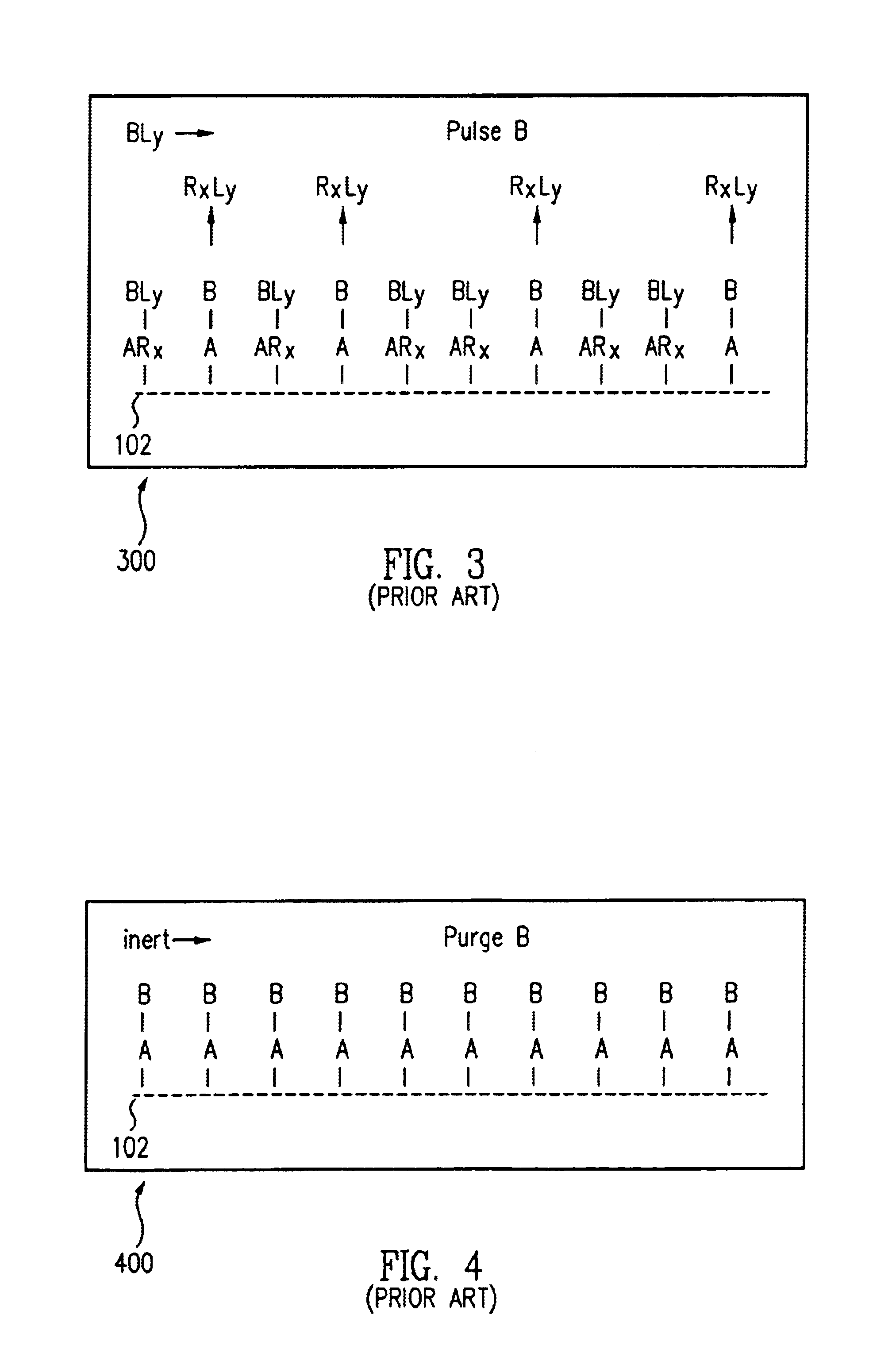
Chemical Vapor Deposition (CVD) and Atomic Layer Deposition (ALD) are thin film deposition techniques used in semiconductor manufacturing. CVD involves the reaction of vapor-phase chemicals on a heated substrate to form solid films, while ALD is characterized by sequential, self-limiting surface reactions that allow for precise atomic-level control of film thickness. These processes differ in their reaction mechanisms, growth rates, and the quality of the resulting films, with ALD typically offering better conformality and uniformity for ultra-thin films.- Fundamental principles and processes of CVD and ALD: Chemical Vapor Deposition (CVD) and Atomic Layer Deposition (ALD) are thin film deposition techniques used in semiconductor manufacturing. CVD involves the reaction of vapor phase chemicals to form solid films, while ALD is characterized by sequential, self-limiting surface reactions that allow for precise atomic-level control of film thickness. These processes differ in their reaction mechanisms, with CVD typically being a continuous process and ALD being a cyclic process with distinct precursor and purge steps.
- Equipment and reactor designs for CVD and ALD processes: Specialized equipment and reactor designs are essential for effective CVD and ALD processes. These include reaction chambers with precise temperature and pressure control, gas delivery systems for precursor transport, and vacuum systems. Advanced reactor designs may incorporate features such as plasma enhancement, rotating substrates, or spatial separation of precursors. The equipment configuration significantly impacts film quality, deposition rate, and process efficiency, with innovations focusing on improved uniformity and reduced contamination.
- Precursor chemistry and material development for thin film deposition: The selection and development of precursor chemicals are critical for successful CVD and ALD processes. Ideal precursors must have sufficient volatility, thermal stability, reactivity, and purity. Research focuses on developing novel precursors for depositing various materials including metals, metal oxides, nitrides, and complex compounds. The precursor chemistry directly influences film properties such as composition, crystallinity, and impurity levels, with recent innovations targeting environmentally friendly alternatives and precursors for new material systems.
- Applications in semiconductor and electronic device manufacturing: CVD and ALD technologies are extensively used in semiconductor and electronic device manufacturing. These processes enable the deposition of high-quality dielectric layers, gate oxides, diffusion barriers, and electrode materials in integrated circuits. They are particularly valuable for creating conformal coatings on high-aspect-ratio structures and 3D architectures in advanced microelectronics. The precise thickness control and excellent conformality of ALD make it especially suitable for nanoscale device fabrication where atomic-level precision is required.
- Process enhancements and hybrid techniques: Various enhancements and hybrid approaches have been developed to overcome limitations of conventional CVD and ALD processes. These include plasma-enhanced CVD (PECVD) and plasma-enhanced ALD (PEALD) that use plasma activation to lower process temperatures and improve film properties. Other innovations include spatial ALD for higher throughput, hot-wire CVD for specific material systems, and combined CVD-ALD processes that leverage advantages of both techniques. These enhanced methods enable deposition of materials with improved properties and expand the range of potential applications.
02 Equipment and reactor designs for CVD and ALD processes
Specialized equipment and reactor designs are crucial for effective CVD and ALD processes. These include reaction chambers with precise temperature and pressure control, gas delivery systems for precursor transport, and vacuum systems. Advanced reactor designs incorporate features such as showerhead distributors for uniform gas flow, rotating substrates for improved film uniformity, and plasma enhancement capabilities. The equipment may also include in-situ monitoring systems to control film growth in real-time and ensure process repeatability.Expand Specific Solutions03 Precursor chemistry and material innovations
The selection and development of precursor chemicals are critical for successful CVD and ALD processes. Ideal precursors must have sufficient volatility, thermal stability, and reactivity for the target application. Recent innovations include the development of metal-organic compounds, halides, and other specialized molecules designed for specific film compositions. Advanced material systems deposited by these techniques include high-k dielectrics, barrier metals, noble metals, and various compound semiconductors, enabling the fabrication of increasingly complex device structures.Expand Specific Solutions04 Applications in semiconductor and electronic device manufacturing
CVD and ALD techniques are extensively used in semiconductor and electronic device manufacturing. These processes enable the deposition of critical layers in integrated circuits, including gate dielectrics, diffusion barriers, electrodes, and interconnects. They are particularly valuable for advanced node technologies requiring precise thickness control and high conformality in high-aspect-ratio structures. These deposition methods also support the fabrication of memory devices, MEMS structures, and various sensors, contributing to continued miniaturization and performance improvements in electronic devices.Expand Specific Solutions05 Process enhancements and hybrid techniques
Various enhancements have been developed to improve CVD and ALD processes, including plasma-enhanced versions (PECVD and PEALD) that allow for lower deposition temperatures and modified film properties. Spatial ALD techniques enable higher throughput by separating precursors spatially rather than temporally. Hybrid approaches combining aspects of both CVD and ALD offer optimized deposition rates while maintaining good film quality. Other innovations include hot-wire CVD, catalytic CVD, and area-selective deposition techniques that enable more precise patterning without additional lithography steps.Expand Specific Solutions
Key Industry Players in Deposition Technology Market
The Chemical Vapor Deposition (CVD) versus Atomic Layer Deposition (ALD) technology landscape is currently in a mature growth phase, with the global market expected to reach $85 billion by 2025. Major semiconductor manufacturers like Samsung Electronics, Micron Technology, and SMIC are driving adoption, while specialized equipment providers such as ASM IP Holding, NAURA Microelectronics, and Nano-Master are advancing technical capabilities. Research institutions including Fudan University and TNO are pushing boundaries in novel applications. The competitive landscape shows ALD gaining momentum for precision nanoscale applications, while CVD maintains dominance in high-throughput scenarios. The technology maturity varies by application, with ALD seeing accelerated adoption in advanced semiconductor nodes where companies like Apple and Samsung Display require atomic-level precision for next-generation devices.
Micron Technology, Inc.
Technical Solution: Micron Technology has developed specialized CVD and ALD processes tailored for advanced memory production. Their CVD technology utilizes optimized precursor delivery systems that enable high-rate deposition of dielectric and conductive films for DRAM and 3D NAND applications. Micron's ALD approach focuses on conformal deposition in high aspect ratio structures (>60:1) with precise thickness control below 1nm. They've pioneered hybrid processes that combine CVD's throughput advantages with ALD's conformality by implementing pulsed CVD techniques. Micron has developed in-situ metrology systems that provide real-time feedback during deposition, enabling adaptive process control. Their comparative studies have shown that while ALD provides superior conformality in deep trenches (>95% step coverage vs 70-80% for CVD), their optimized CVD processes achieve 3-4x higher throughput for certain applications. Micron's technology roadmap indicates a strategic shift toward ALD for critical layers as device dimensions continue to shrink below 10nm[5][6].
Strengths: Optimized processes for memory-specific applications; advanced in-situ monitoring capabilities; effective balance between throughput and quality; strong integration with other process steps. Weaknesses: Less versatility for non-memory applications; higher operational costs for ALD processes; complex precursor management systems required.
Samsung Electronics Co., Ltd.
Technical Solution: Samsung Electronics has developed proprietary ALD and CVD technologies optimized for advanced memory and logic device fabrication. Their ALD approach employs thermal and plasma-enhanced processes to deposit high-k dielectrics and metal gates with exceptional conformality in 3D NAND structures with aspect ratios exceeding 100:1. Samsung's CVD technology focuses on high-throughput deposition of silicon nitride, silicon oxide, and metal films using precursor engineering to enhance film properties. The company has pioneered area-selective deposition techniques that combine aspects of both ALD and CVD to enable self-aligned processes, reducing lithography steps. Samsung's integrated approach allows switching between ALD and CVD modes within the same chamber, optimizing cycle time and cost. Their research has demonstrated that ALD provides 30% better step coverage in DRAM capacitor structures while CVD offers 2-3x higher deposition rates for certain materials[3][4].
Strengths: Comprehensive expertise in both technologies; highly optimized processes for memory manufacturing; advanced precursor development capabilities; excellent integration with other fabrication steps. Weaknesses: Proprietary technologies may limit compatibility with third-party equipment; higher capital investment requirements; complex process control systems needed for optimization.
Critical Technical Innovations in Deposition Processes
Atomic layer deposition methods and chemical vapor deposition methods
PatentInactiveUS7488386B2
Innovation
- The method involves chemisorbing a precursor material on a substrate without exposing it to microwave radiation, followed by exposing the chemisorbed material to microwave radiation within the reaction chamber, allowing for the use of thermally unstable precursors by controlling thermal energy during the deposition process.
Atomic layer deposition systems and methods
PatentInactiveUS6902620B1
Innovation
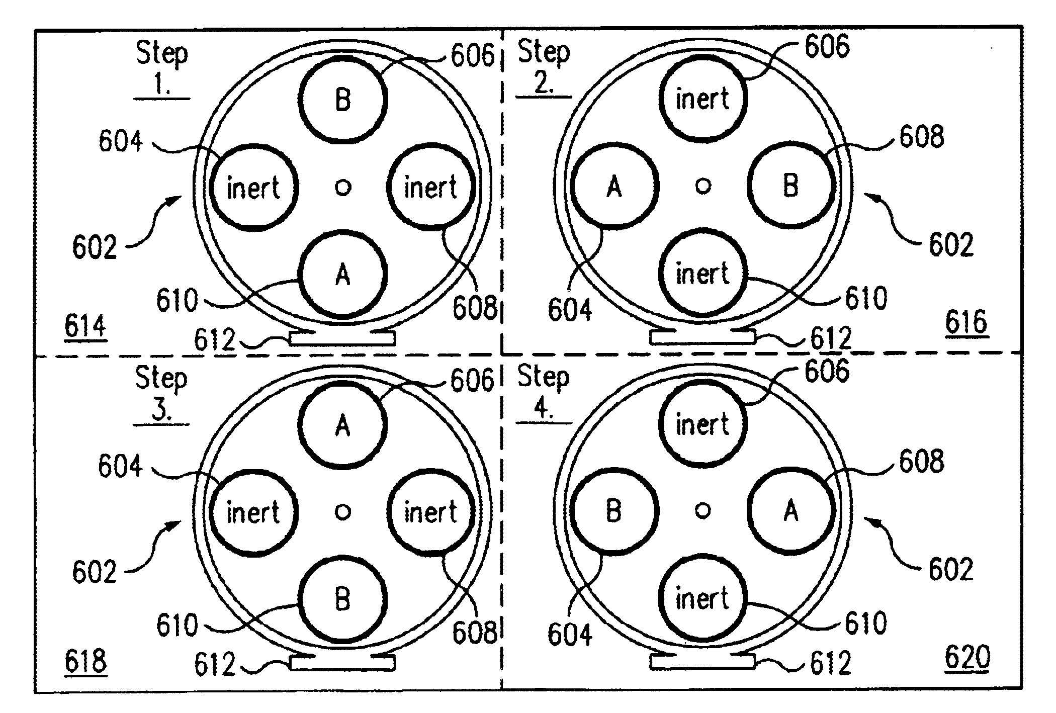
- Implementing a multi-wafer sequential processing system with rotary gas switching, allowing for concurrent ALD and CVD processing, where wafers are rotated through multiple stations with sequential gas introduction and inert gas purging to prevent intermixing, enabling efficient deposition of thin films across multiple wafers simultaneously.
Environmental Impact and Sustainability Considerations
The environmental footprint of thin film deposition technologies has become increasingly important as industries face stricter regulations and growing sustainability concerns. Chemical Vapor Deposition (CVD) and Atomic Layer Deposition (ALD) differ significantly in their environmental impacts across multiple dimensions, with implications for sustainable manufacturing practices.
CVD processes typically require higher operating temperatures (600-1000°C) compared to ALD (200-350°C), resulting in substantially higher energy consumption. This temperature differential translates to approximately 30-50% greater energy usage for CVD operations, contributing to larger carbon footprints in manufacturing facilities. Additionally, CVD's continuous flow process often leads to precursor utilization efficiencies of only 5-15%, whereas ALD's self-limiting reactions achieve 80-95% efficiency.
Waste generation represents another critical environmental consideration. CVD systems produce significant gaseous byproducts and particulate matter requiring extensive abatement systems. Studies indicate CVD processes generate 3-5 times more waste gases per unit of film deposited compared to ALD. The latter's precise monolayer deposition mechanism minimizes chemical waste and reduces the need for post-process cleaning chemicals.
Precursor chemicals used in both technologies present varying degrees of environmental hazard. Traditional CVD often employs metal-organic compounds containing toxic elements like mercury, lead, or cadmium. While ALD also utilizes reactive chemicals, its precise dosing requirements have driven development of less hazardous alternatives and "green chemistry" precursors with reduced environmental persistence.
Water consumption patterns differ markedly between these technologies. CVD cooling systems typically require 2-3 times more water than comparable ALD installations due to higher operating temperatures and continuous operation. Some advanced ALD systems have implemented closed-loop cooling that reduces water consumption by up to 80% compared to conventional approaches.
From a lifecycle perspective, ALD equipment generally demonstrates longer operational lifespans with fewer component replacements, reducing manufacturing waste. However, the slower deposition rates of ALD can necessitate more equipment units to achieve equivalent production volumes, potentially offsetting some sustainability advantages through increased manufacturing resource requirements.
Recent industry initiatives have focused on developing hybrid approaches that combine the throughput advantages of CVD with the precision and efficiency of ALD, potentially offering optimized environmental performance. These developments, alongside advances in precursor chemistry and energy recovery systems, suggest a trajectory toward significantly reduced environmental impacts for both technologies in coming years.
Cost-Benefit Analysis of CVD vs ALD Implementation
When evaluating the implementation of Chemical Vapor Deposition (CVD) versus Atomic Layer Deposition (ALD) technologies, a comprehensive cost-benefit analysis reveals significant differences that impact manufacturing decisions across various industries.
Initial capital investment represents a primary consideration, with CVD systems typically requiring 30-50% lower upfront costs compared to ALD equipment. Standard CVD reactors range from $200,000 to $800,000, while comparable ALD systems often command $400,000 to $1.5 million due to their more sophisticated precursor delivery systems and control mechanisms. However, this initial cost advantage for CVD diminishes when considering total cost of ownership.
Operational expenses reveal a more nuanced picture. CVD processes generally consume 40-60% more precursor materials than ALD, resulting in higher ongoing material costs. Energy consumption also favors ALD, which typically requires 25-35% less power due to lower operating temperatures and more efficient precursor utilization. Maintenance costs for CVD systems average 15-20% higher annually, primarily due to more frequent chamber cleaning requirements and component replacements.
Production efficiency metrics demonstrate ALD's advantages in certain applications. While CVD offers faster deposition rates (typically 10-100 nm/min versus ALD's 0.1-1 nm/min), ALD provides superior film uniformity with deviation typically below 1%, compared to CVD's 3-5%. This translates to higher yields in precision applications, with ALD demonstrating 5-15% better yield rates for complex high-aspect-ratio structures.
Return on investment calculations indicate that despite higher initial costs, ALD systems typically achieve break-even points within 2-4 years in high-precision manufacturing environments. This is primarily driven by material savings, reduced rework rates, and higher yields. Conversely, CVD maintains ROI advantages in less demanding applications where throughput is prioritized over atomic-level precision.
Industry-specific analyses reveal varying cost-benefit profiles. In semiconductor manufacturing, ALD's precision justifies its premium for sub-10nm nodes, while traditional CVD remains cost-effective for larger feature sizes. In optical coating applications, ALD's superior uniformity delivers 20-30% longer product lifespans, offsetting higher production costs. The medical device sector increasingly favors ALD for implantable devices due to reduced defect rates, despite 30-40% higher processing costs.
Future economic projections suggest narrowing cost differentials as ALD technology matures and economies of scale improve. Emerging hybrid systems combining CVD and ALD capabilities may offer optimized cost-benefit profiles for specific applications, potentially reshaping implementation decisions across manufacturing sectors.
Unlock deeper insights with Patsnap Eureka Quick Research — get a full tech report to explore trends and direct your research. Try now!
Generate Your Research Report Instantly with AI Agent
Supercharge your innovation with Patsnap Eureka AI Agent Platform!