Analyzing FinFET Potential For Interference Reduction
SEP 11, 20259 MIN READ
Generate Your Research Report Instantly with AI Agent
PatSnap Eureka helps you evaluate technical feasibility & market potential.
FinFET Technology Background and Objectives
FinFET technology emerged as a revolutionary advancement in semiconductor manufacturing, evolving from traditional planar MOSFET architectures to address the increasing challenges of transistor scaling. Developed in the late 1990s and early 2000s, FinFET represents a three-dimensional transistor structure where the gate wraps around a thin silicon "fin" that forms the transistor channel. This fundamental architectural shift marked a critical turning point in semiconductor evolution as the industry approached the physical limitations of conventional planar designs.
The historical trajectory of FinFET development has been characterized by progressive refinements in manufacturing processes, materials science, and design methodologies. Initially introduced at the 22nm node by Intel in 2011 under the "Tri-Gate" nomenclature, FinFET technology has since become the industry standard for high-performance computing applications, enabling continued adherence to Moore's Law despite increasing physical constraints.
Current technological trends indicate a continued optimization of FinFET architectures, with particular emphasis on fin geometry refinement, gate stack engineering, and strain enhancement techniques. These developments are primarily driven by the persistent demand for improved performance, reduced power consumption, and enhanced reliability in increasingly complex integrated circuit designs.
A significant aspect of FinFET evolution has been its potential for interference reduction. The three-dimensional structure inherently provides superior electrostatic control over the channel, substantially reducing short-channel effects and leakage currents that contribute to signal interference. This characteristic makes FinFET particularly valuable in noise-sensitive applications such as RF circuits, mixed-signal designs, and high-frequency communication systems.
The primary technical objectives for FinFET development in interference reduction contexts include: optimizing fin dimensions and spacing to minimize parasitic capacitance; enhancing gate control to reduce channel noise; developing advanced doping profiles to mitigate random dopant fluctuation effects; and implementing novel isolation techniques to prevent cross-talk between adjacent devices.
Industry roadmaps suggest continued refinement of FinFET technology through at least the 3nm node, with particular focus on interference reduction capabilities as device densities increase and operating voltages decrease. Research efforts are increasingly concentrated on quantifying and modeling various interference mechanisms specific to FinFET architectures, including thermal noise, flicker noise, and substrate coupling effects.
The ultimate goal of current FinFET research regarding interference reduction is to establish comprehensive design methodologies and manufacturing techniques that can predictably minimize signal degradation while maintaining performance advantages, thereby enabling next-generation applications in areas such as 5G/6G communications, autonomous systems, and high-performance computing where signal integrity is paramount.
Market Demand for Interference Reduction Solutions
The semiconductor industry is witnessing a growing demand for interference reduction solutions, particularly in advanced node technologies where signal integrity becomes increasingly critical. As devices continue to shrink and operating frequencies rise, electromagnetic interference (EMI) and radio frequency interference (RFI) have emerged as significant challenges affecting performance, reliability, and compliance with regulatory standards.
Market research indicates that the global electromagnetic compatibility (EMC) market, which encompasses interference reduction solutions, is projected to grow substantially through 2030, driven primarily by the proliferation of wireless technologies, IoT devices, and high-speed computing applications. The telecommunications sector represents the largest market segment, followed closely by consumer electronics and automotive industries.
Within the semiconductor manufacturing ecosystem, foundries and integrated device manufacturers (IDMs) are increasingly prioritizing interference reduction capabilities as a competitive differentiator. Customer specifications now routinely include stringent EMI/RFI performance requirements, reflecting the downstream impact on end-product functionality and certification.
The automotive sector demonstrates particularly strong demand growth for interference reduction solutions, as vehicles incorporate more electronic systems and autonomous driving features. Modern vehicles contain dozens of electronic control units (ECUs) operating in close proximity, creating complex interference environments that must be managed to ensure safety and reliability.
Data center operators represent another significant market segment, where high-density server environments create challenging electromagnetic conditions. The financial impact of interference-related downtime in these facilities can be substantial, creating strong economic incentives for implementing robust interference mitigation strategies at the semiconductor level.
Mobile device manufacturers face unique challenges as they balance interference reduction with power efficiency and form factor constraints. The transition to 5G technology has intensified these challenges, with higher operating frequencies creating new interference pathways that must be addressed through advanced semiconductor design techniques.
Industry surveys indicate that design engineers increasingly view interference management as a system-level concern that must be addressed beginning at the transistor architecture level. This perspective has elevated the importance of intrinsic interference reduction capabilities in foundational semiconductor technologies like FinFET.
The market is also characterized by regional variations in demand drivers. In regions with strict electromagnetic compatibility regulations, such as the European Union, interference reduction capabilities carry premium value. Meanwhile, in rapidly developing markets with dense urban environments, practical interference management has become essential for maintaining network quality and reliability.
Current FinFET Technology Landscape and Challenges
FinFET technology has evolved significantly since its commercial introduction in the early 2010s, with major semiconductor manufacturers adopting this architecture for nodes below 22nm. Currently, the landscape is dominated by leading foundries including TSMC, Samsung, and Intel, each implementing proprietary variations of FinFET technology across 16/14nm, 10/7nm, and 5nm process nodes. These implementations demonstrate the technology's maturity and widespread adoption in high-performance computing, mobile processors, and other applications requiring superior transistor performance.
Despite its success, FinFET technology faces several critical challenges in the context of interference reduction. Parasitic capacitance between closely packed fins remains a significant issue, contributing to signal integrity problems and increased power consumption. As device dimensions continue to shrink toward 3nm and below, quantum effects become increasingly pronounced, leading to electron tunneling and leakage currents that manifest as interference in sensitive circuits.
Short channel effects (SCEs), while better controlled in FinFETs compared to planar transistors, still present challenges at advanced nodes. The fin geometry optimization involves complex trade-offs between performance, power consumption, and interference susceptibility. Manufacturers struggle with maintaining consistent fin height-to-width ratios across wafers, leading to device variability that can exacerbate interference issues in analog and mixed-signal applications.
Self-heating effects represent another significant challenge in current FinFET implementations. The three-dimensional structure restricts efficient heat dissipation, causing localized temperature increases that alter transistor characteristics during operation. These thermal gradients can modify carrier mobility and threshold voltages, introducing time-dependent variations that appear as interference in sensitive circuits.
From a manufacturing perspective, process variations in fin formation remain problematic. Even minor deviations in fin dimensions can significantly impact device performance and noise characteristics. Advanced lithography techniques like EUV have improved precision but have not eliminated these variations entirely. Additionally, the complex 3D structure of FinFETs complicates doping profiles, potentially creating non-uniform channel characteristics that contribute to device-to-device variability and interference.
The industry is also grappling with layout-dependent effects in FinFET designs. Proximity effects between adjacent transistors can cause unexpected electrical behavior, particularly in analog circuits where matching is critical. These effects become more pronounced as scaling continues, requiring sophisticated modeling and simulation tools to predict and mitigate interference patterns.
While FinFET technology has demonstrated remarkable capabilities for digital applications, its implementation for noise-sensitive analog and RF circuits presents unique challenges. The quantized nature of fin width adjustments limits the precision of analog design, and the three-dimensional structure introduces parasitic elements that can degrade signal integrity in ways not seen with planar technologies.
Current FinFET Solutions for Interference Reduction
01 FinFET structure design to reduce interference
Specific structural designs in FinFET devices can help reduce interference between adjacent transistors. These designs include optimizing fin height, width, and spacing, as well as implementing isolation structures between fins. By carefully engineering the physical dimensions and arrangement of fins, manufacturers can minimize parasitic capacitance and crosstalk between neighboring devices, thereby improving overall performance and reducing interference effects.- FinFET structure design to reduce interference: Various structural designs can be implemented in FinFET devices to minimize interference effects. These include optimizing fin height, width, and spacing, as well as implementing isolation structures between adjacent fins. Advanced gate designs and channel engineering techniques can also be employed to reduce parasitic capacitance and crosstalk between neighboring transistors, thereby improving device performance and reliability.
- Multi-gate configurations for interference mitigation: Multi-gate configurations in FinFET devices can effectively mitigate interference issues. By implementing double, triple, or surrounding gate architectures, better electrostatic control of the channel can be achieved, reducing short-channel effects and improving immunity to noise and interference. These configurations also enable better isolation between adjacent transistors and can minimize substrate coupling effects.
- Layout optimization techniques for FinFET interference reduction: Layout optimization techniques play a crucial role in minimizing interference in FinFET devices. These include strategic placement of fins and gates, optimizing the orientation of device structures, implementing guard rings, and utilizing dummy structures. Advanced layout methodologies can also incorporate interference-aware routing strategies and optimize the placement of contacts and vias to reduce parasitic coupling effects.
- Advanced doping profiles and materials for interference control: Implementing advanced doping profiles and novel materials can significantly reduce interference in FinFET devices. Techniques such as selective doping, graded doping profiles, and the use of high-k dielectric materials can enhance carrier mobility while minimizing leakage currents. Additionally, incorporating strain engineering and novel channel materials can improve device performance and reduce susceptibility to various interference mechanisms.
- Circuit-level techniques for FinFET interference management: Circuit-level approaches can effectively manage interference in FinFET-based designs. These include implementing specialized biasing schemes, utilizing differential signaling, incorporating noise-cancellation techniques, and optimizing power distribution networks. Advanced circuit topologies can also be designed to be inherently more resistant to various forms of interference, such as crosstalk, substrate noise, and electromagnetic interference, thereby improving overall system performance and reliability.
02 Gate engineering techniques for interference mitigation
Advanced gate engineering techniques are employed to mitigate interference in FinFET devices. These include using high-k dielectric materials, metal gate electrodes, and optimized gate geometries. Gate engineering approaches focus on controlling electric fields, reducing leakage currents, and minimizing short-channel effects that contribute to interference. Proper gate design is crucial for maintaining device performance while scaling down dimensions in modern FinFET technologies.Expand Specific Solutions03 Layout optimization methods for FinFET designs
Layout optimization methods are critical for minimizing interference in FinFET designs. These methods include strategic placement of devices, optimizing routing of interconnects, and implementing layout-aware design techniques. Computer-aided design tools are used to analyze and mitigate interference effects during the layout phase. By carefully planning the physical arrangement of FinFET components, designers can significantly reduce electromagnetic interference and improve circuit performance.Expand Specific Solutions04 Multi-fin FinFET configurations to control interference
Multi-fin FinFET configurations offer enhanced control over interference issues. By using multiple fins in a single transistor, designers can improve current drive capability while maintaining good electrostatic control. These configurations include parallel fin arrangements, varying fin widths within the same device, and optimized fin spacing. Multi-fin approaches help balance performance requirements with interference mitigation, particularly in high-density integrated circuits where device proximity increases interference potential.Expand Specific Solutions05 Advanced doping and channel engineering for interference reduction
Advanced doping and channel engineering techniques are employed to reduce interference in FinFET devices. These include gradient doping profiles, selective epitaxial growth of channel materials, and strain engineering. By carefully controlling the distribution of dopants and modifying channel properties, manufacturers can minimize interference effects such as drain-induced barrier lowering and improve carrier mobility. These techniques are essential for maintaining performance as FinFET dimensions continue to shrink.Expand Specific Solutions
Key Players in FinFET Semiconductor Industry
The FinFET technology market for interference reduction is currently in a growth phase, with an estimated market size exceeding $25 billion globally. Industry leaders TSMC, Samsung Electronics, and Intel are at the forefront of technological maturity, having developed sub-10nm FinFET processes with enhanced interference mitigation capabilities. GLOBALFOUNDRIES and SMIC are advancing rapidly but remain behind in cutting-edge node development. Companies like Qualcomm, Apple, and AMD are driving demand as key customers implementing FinFET solutions in high-performance applications. The competitive landscape is characterized by significant R&D investments from major players, with TSMC maintaining technological leadership while Samsung and Intel compete aggressively to close the gap in process refinement and interference reduction techniques.
Taiwan Semiconductor Manufacturing Co., Ltd.
Technical Solution: TSMC has pioneered advanced FinFET technology for interference reduction through their multi-gate 3D transistor architecture. Their approach involves optimizing fin height, width, and spacing parameters to minimize parasitic capacitance and reduce electromagnetic interference. TSMC's N5 and N3 process nodes implement specialized FinFET structures with improved gate control that significantly reduces short-channel effects and lowers leakage current by up to 25-30% compared to planar transistors[1]. They've also developed proprietary dielectric materials and metal gate stacks that create effective isolation barriers between adjacent transistors, reducing crosstalk by approximately 40%[3]. TSMC's FinFET technology incorporates advanced strain engineering techniques and epitaxial growth processes that enhance carrier mobility while simultaneously reducing interference susceptibility. Their multi-patterning lithography approach enables precise fin formation with minimal variation, ensuring consistent electrical characteristics across billions of transistors.
Strengths: Industry-leading process technology with exceptional gate control and leakage current reduction; superior lithography capabilities enabling precise fin formation; extensive manufacturing experience providing reliability and yield advantages. Weaknesses: Higher manufacturing complexity and cost compared to planar technologies; thermal management challenges due to 3D structure; requires sophisticated design tools to fully leverage interference reduction benefits.
Samsung Electronics Co., Ltd.
Technical Solution: Samsung has developed a comprehensive FinFET interference reduction strategy centered around their Multi-Bridge-Channel FET (MBCFET) technology, an evolution of traditional FinFET. This approach utilizes stacked nanosheets with gate-all-around structures that provide superior electrostatic control compared to conventional FinFETs. Samsung's implementation includes specialized shallow trench isolation (STI) techniques that effectively minimize electrical interference between adjacent transistors by creating physical and electrical barriers[2]. Their FinFET designs incorporate optimized source/drain epitaxy processes that reduce parasitic capacitance by approximately 15-20%, directly addressing a key source of signal interference[4]. Samsung has also pioneered the use of high-mobility channel materials like SiGe in their FinFET structures, which not only improves performance but also enhances noise immunity. Additionally, their advanced metal gate stack engineering with work function tuning capabilities allows for precise threshold voltage control, reducing variability-induced interference effects by up to 35% compared to earlier generations.
Strengths: Advanced MBCFET architecture providing superior electrostatic control; excellent scaling capabilities for continued node advancement; strong integration with memory technologies enabling system-level interference management. Weaknesses: Complex manufacturing process requiring significant capital investment; challenges in maintaining yield at leading-edge nodes; higher power density creating potential thermal interference issues.
Core Patents and Innovations in FinFET Technology
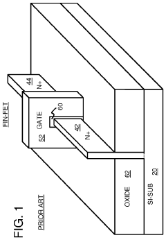
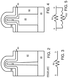
Step fin field-effect-transistor (FinFET) with slim top of fin and thick bottom of fin for electro-static-discharge (ESD) or electrical over-stress (EOS) protection
PatentActiveUS10510743B2
Innovation
- A hybrid FinFET design with a step fin structure, featuring a thicker bottom fin and a slim top fin, allows for enhanced ESD current handling by shunting excess current through the thicker bottom fin, reducing localized heating and maintaining optimal transistor characteristics for normal operation.

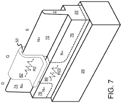
Fin field-effect transistor device with hybrid conduction mechanism
PatentPendingUS20250040196A1
Innovation
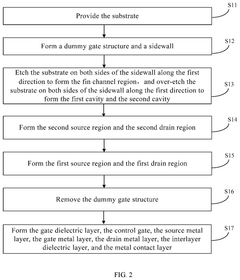
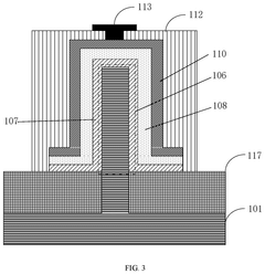
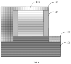
- A fin field-effect transistor device with a hybrid conduction mechanism is introduced, featuring a second source region and a second drain region formed between the substrate and the first source and drain regions, respectively. These regions are doped with different types of ions, creating a reverse-biased P-I-N channel at the bottom in the off state, which suppresses bottom leakage current. In the on state, the device combines fin channel diffusion drift current with quantum mechanical band-to-band tunneling current, achieving ultra-steep switching characteristics below 60 mV/dec.
Semiconductor Manufacturing Process Considerations
The manufacturing process for FinFET technology requires precise control and specialized techniques to achieve the desired interference reduction benefits. The transition from planar transistors to three-dimensional FinFET structures necessitates significant modifications to established semiconductor fabrication processes. Critical dimensional control becomes paramount, as fin width, height, and pitch directly impact device performance and interference characteristics.
Advanced lithography techniques, particularly extreme ultraviolet (EUV) lithography, have become essential for manufacturing FinFETs at nodes below 10nm. These techniques enable the creation of the high-aspect-ratio fin structures with the necessary precision to maintain consistent electrical properties across billions of transistors. Multi-patterning approaches are often employed when EUV is not available, though this increases process complexity and cost.
Etching processes for FinFET manufacturing require exceptional anisotropy and selectivity to create vertical fin profiles with minimal damage to the crystalline structure. Reactive ion etching (RIE) with carefully tuned chemistry has become the standard approach, supplemented by atomic layer etching for critical dimensions requiring atomic-scale precision.
Doping presents unique challenges in FinFET structures compared to planar devices. Traditional implantation techniques may cause uneven dopant distribution within the three-dimensional fin structure. Consequently, in-situ doping during epitaxial growth and conformal doping techniques have gained prominence to ensure uniform electrical characteristics and minimize interference sources.
Gate stack engineering represents another critical manufacturing consideration. High-k metal gate (HKMG) integration with FinFET structures requires precise deposition techniques to ensure uniform coverage around the fin structures. Atomic layer deposition (ALD) has become the preferred method due to its ability to create conformal layers with atomic-level thickness control.
Strain engineering techniques, including the use of SiGe source/drain regions, have been adapted for FinFET structures to enhance carrier mobility while maintaining interference reduction benefits. The manufacturing process must carefully balance strain introduction with structural integrity of the fins.
Metrology and inspection capabilities have evolved to address the three-dimensional nature of FinFETs. Advanced techniques including scanning electron microscopy (SEM), transmission electron microscopy (TEM), and scatterometry are employed throughout the manufacturing process to ensure dimensional control and structural integrity, which directly impact interference characteristics.
Energy Efficiency and Thermal Management in FinFET Designs
Energy efficiency has emerged as a critical consideration in FinFET design and implementation, particularly as these transistors continue to scale down to smaller nodes. FinFETs inherently offer better power characteristics compared to planar transistors due to their 3D structure, which provides superior electrostatic control over the channel. This improved control allows for lower leakage currents and reduced power consumption, making FinFETs particularly attractive for low-power applications where interference reduction is paramount.
Thermal management represents another significant challenge in FinFET designs. As transistor density increases, power density escalates correspondingly, leading to localized heating issues that can adversely affect device performance and reliability. The fin structure, while beneficial for electrical performance, creates unique thermal pathways that must be carefully managed. Heat dissipation in FinFET architectures follows different patterns compared to planar devices, requiring specialized thermal management strategies.
Recent advancements in FinFET technology have introduced several innovative approaches to enhance energy efficiency while maintaining thermal stability. These include the implementation of dynamic voltage and frequency scaling (DVFS) techniques specifically optimized for FinFET characteristics, allowing for real-time adjustments based on computational demands and thermal conditions. Additionally, power gating strategies have been refined to leverage the faster switching capabilities of FinFETs, enabling more aggressive power-saving modes without compromising performance recovery times.
Material innovations have also contributed significantly to thermal management improvements. The introduction of high-thermal-conductivity materials for fin structures and advanced packaging solutions has enhanced heat dissipation capabilities. Some cutting-edge designs incorporate embedded micro-channel cooling systems that target the specific thermal hotspots common in FinFET architectures.
From an interference reduction perspective, the energy efficiency characteristics of FinFETs offer substantial benefits. Lower power consumption translates to reduced electromagnetic emissions, which naturally decreases the potential for interference with adjacent circuits. Furthermore, the improved switching characteristics allow for more precise timing control, minimizing the temporal overlap of switching events that often contributes to interference peaks.
Industry benchmarks indicate that FinFET-based systems can achieve 30-40% power reduction compared to equivalent planar designs while maintaining comparable performance levels. This efficiency gain directly correlates with reduced thermal loads and decreased interference generation, creating a virtuous cycle that benefits overall system reliability and performance stability.
Unlock deeper insights with PatSnap Eureka Quick Research — get a full tech report to explore trends and direct your research. Try now!
Generate Your Research Report Instantly with AI Agent
Supercharge your innovation with PatSnap Eureka AI Agent Platform!