Enhancing FinFET Performance For Augmented Reality
SEP 11, 202510 MIN READ
Generate Your Research Report Instantly with AI Agent
PatSnap Eureka helps you evaluate technical feasibility & market potential.
FinFET Evolution and AR Performance Goals
FinFET technology has undergone significant evolution since its introduction in the early 2000s. Initially developed to address the scaling limitations of planar transistors, FinFETs have become the cornerstone of modern semiconductor manufacturing. The three-dimensional fin structure allows for better electrostatic control of the channel, reducing leakage current and enabling continued device scaling beyond the 22nm node. This architectural advantage has positioned FinFETs as the dominant transistor technology in high-performance computing applications for over a decade.
The progression of FinFET technology has been marked by several key milestones. First-generation FinFETs featured relatively simple fin structures with limited performance optimization. Subsequent generations introduced innovations such as strain engineering, high-k metal gates, and epitaxial source/drain regions, each contributing to enhanced carrier mobility and reduced parasitic resistances. Recent advancements have focused on fin shape optimization, novel channel materials, and contact resistance reduction techniques to further improve performance metrics.
For augmented reality (AR) applications, FinFET performance goals are particularly demanding due to the unique computational requirements of AR systems. These systems must process complex visual data, perform spatial mapping, and render graphics with minimal latency while operating within strict power constraints of wearable devices. Specifically, AR processors require high computing throughput for real-time image processing, machine learning acceleration for object recognition, and efficient power management to extend battery life in compact form factors.
The technical objectives for FinFETs in AR contexts include achieving sub-0.5V operation for ultra-low power consumption, transistor switching speeds below 10 picoseconds to support high-frequency operation, and significantly reduced device variability to ensure consistent performance across millions of transistors. Additionally, thermal management has emerged as a critical concern, necessitating innovations in heat dissipation techniques specific to the confined spaces of AR headsets and glasses.
Looking forward, the roadmap for FinFET evolution in AR applications is focusing on several promising directions. These include the integration of novel channel materials such as germanium and III-V compounds to enhance carrier mobility, the development of vertical transport FinFETs for increased current density, and the exploration of hybrid architectures that combine FinFETs with emerging technologies like nanosheet transistors to optimize the performance-power envelope.
The convergence of FinFET technology advancement and AR performance requirements represents a significant opportunity for innovation. Success in this domain will require interdisciplinary approaches that consider not only transistor-level optimizations but also system-level architectural decisions that leverage the unique characteristics of FinFET technology to address the specific computational patterns of AR workloads.
AR Market Demands for Advanced Semiconductor Solutions
The augmented reality (AR) market is experiencing unprecedented growth, creating significant demands for advanced semiconductor solutions. Current market projections indicate that the global AR market will reach $70 billion by 2023, with a compound annual growth rate of approximately 43%. This explosive growth is driving semiconductor manufacturers to develop increasingly powerful, energy-efficient chips capable of handling AR's intensive computational requirements.
AR applications demand exceptional processing capabilities to deliver seamless real-time experiences. Users expect instantaneous environmental mapping, object recognition, and digital overlay rendering without noticeable latency. Market research shows that consumers abandon AR applications when experiencing delays exceeding 100 milliseconds, highlighting the critical need for high-performance semiconductors.
Power efficiency represents another crucial market requirement. As AR devices transition from tethered systems to standalone wearables, battery life becomes a primary concern. Industry surveys reveal that consumers expect AR glasses to function for at least 8 hours on a single charge while maintaining full functionality. This creates direct pressure on semiconductor manufacturers to enhance FinFET performance while reducing power consumption.
Thermal management presents a significant challenge in AR hardware design. Wearable AR devices must maintain comfortable operating temperatures despite intensive processing demands. Market analysis indicates that devices exceeding 35°C surface temperature face significant consumer resistance, creating demand for semiconductor solutions that generate less heat while maintaining performance.
Form factor considerations further drive semiconductor innovation. The market increasingly favors sleek, lightweight AR glasses over bulky headsets. This trend necessitates smaller, more efficient semiconductor components. Industry experts predict that successful AR glasses must weigh under 70 grams to achieve mass market adoption, placing additional constraints on semiconductor design and performance.
The enterprise sector represents a particularly promising market segment for advanced AR semiconductors. Industries including manufacturing, healthcare, and logistics are implementing AR solutions to improve operational efficiency. These applications require industrial-grade reliability and performance under varied environmental conditions, creating demand for specialized semiconductor solutions with enhanced durability and consistent performance across temperature ranges.
Security requirements also shape market demands for AR semiconductors. As AR applications access increasingly sensitive personal and corporate data, hardware-level security features become essential. Market research indicates that 78% of enterprise customers consider robust security capabilities a prerequisite for AR technology adoption, driving demand for advanced security features integrated directly into semiconductor architecture.
FinFET Technology Status and Challenges for AR Applications
FinFET technology has evolved significantly over the past decade, becoming the cornerstone of modern semiconductor manufacturing processes. Currently, FinFET architectures dominate high-performance computing applications with their superior electrostatic control and reduced short-channel effects compared to planar transistors. For augmented reality (AR) applications specifically, the global landscape shows varying levels of technological maturity, with major semiconductor hubs in the United States, Taiwan, South Korea, and increasingly China developing specialized FinFET variants.
The current state of FinFET technology for AR applications faces several critical challenges. Power efficiency remains paramount as AR devices require extended battery life while maintaining high computational performance. Standard FinFET designs struggle to meet the ultra-low power requirements while delivering the necessary processing capabilities for real-time AR rendering and spatial computing.
Thermal management presents another significant hurdle, as AR headsets and glasses have strict thermal constraints due to their proximity to users' faces. Traditional FinFET architectures generate considerable heat under high computational loads, necessitating advanced cooling solutions or architectural modifications to maintain user comfort and device reliability.
Dimensional scaling has reached physical limitations around 3nm, creating challenges for further miniaturization. This is particularly problematic for AR applications where component size directly impacts device form factor and wearability. The industry is exploring vertical scaling and novel materials to overcome these physical barriers.
Integration complexity represents another major challenge, as AR systems require heterogeneous integration of various components including sensors, displays, and processors. Current FinFET manufacturing processes are not fully optimized for such complex system-on-chip designs that combine analog, RF, and digital circuits.
From a geographical perspective, Taiwan leads FinFET manufacturing capabilities through TSMC's advanced nodes, while Samsung and Intel compete with their own FinFET variants. Research institutions in Europe and Japan are focusing on material innovations to enhance FinFET performance specifically for low-power applications relevant to AR.
The technical constraints are further complicated by yield issues at advanced nodes below 5nm, which increases production costs and limits mass adoption in consumer AR devices. Additionally, the industry faces challenges in balancing performance requirements with power constraints, as AR applications demand both high computational throughput and energy efficiency simultaneously.
Radiation sensitivity and reliability concerns also emerge as FinFET dimensions shrink, potentially affecting the long-term stability of AR devices, especially those intended for outdoor use where environmental factors play a significant role in device performance and longevity.
Current FinFET Solutions for AR Processing Requirements
01 FinFET structure optimization
Optimizing the physical structure of FinFETs can significantly enhance their performance. This includes modifications to fin dimensions, shape, and spacing. By carefully engineering the fin height, width, and pitch, manufacturers can achieve better current drive capabilities and reduced short-channel effects. Additionally, optimizing the gate structure around the fin and implementing multi-fin configurations can lead to improved electrical characteristics and overall device performance.- FinFET structure optimization: Optimizing the physical structure of FinFETs can significantly enhance their performance. This includes modifications to fin dimensions, shape, and spacing to improve carrier mobility and reduce parasitic capacitance. Structural innovations such as multi-fin configurations and fin height adjustments can lead to better current drive capabilities while maintaining low leakage. These structural optimizations are fundamental to achieving higher performance in FinFET devices.
- Gate engineering techniques: Advanced gate engineering techniques are crucial for enhancing FinFET performance. These include implementing high-k metal gate materials, optimizing gate length, and developing novel gate stack configurations. Gate work function tuning allows for threshold voltage adjustment, while gate-all-around designs provide better electrostatic control. These techniques help minimize short channel effects and improve switching characteristics, resulting in faster and more energy-efficient FinFET devices.
- Source/drain modifications: Enhancing source and drain regions through epitaxial growth, strain engineering, and advanced doping profiles can significantly improve FinFET performance. Techniques such as selective epitaxial growth of SiGe or SiC in source/drain regions introduce beneficial strain that enhances carrier mobility. Optimized doping gradients and reduced contact resistance at source/drain interfaces help minimize parasitic resistance, leading to improved current drive and switching speed in FinFET devices.
- Channel engineering and strain techniques: Channel engineering techniques focus on enhancing carrier transport properties within the FinFET channel. This includes implementing strain engineering through various methods such as embedded stressors, stress liners, or substrate orientation selection. Channel material modifications, such as incorporating germanium or III-V materials, can significantly improve carrier mobility. These approaches effectively enhance the intrinsic performance of FinFETs by optimizing the fundamental carrier transport mechanisms in the channel region.
- Design and simulation methodologies: Advanced design and simulation methodologies are essential for optimizing FinFET performance. Computational approaches enable accurate modeling of device physics, parasitic effects, and reliability concerns before fabrication. Design techniques include layout optimization, process variation analysis, and performance-power trade-off evaluations. These methodologies help identify optimal device parameters and circuit configurations, allowing for systematic performance improvements while addressing manufacturing constraints and reliability requirements.
02 Strain engineering techniques
Strain engineering is a critical approach to enhance FinFET performance by modifying the semiconductor crystal lattice to improve carrier mobility. Various techniques include applying tensile or compressive stress to the channel region, incorporating epitaxial source/drain regions with different lattice constants, and using stress memorization techniques. These methods can significantly increase electron and hole mobility, resulting in faster switching speeds and improved current drive capabilities in FinFET devices.Expand Specific Solutions03 Gate stack engineering
Advanced gate stack engineering is essential for optimizing FinFET performance. This includes the selection of high-k dielectric materials, metal gate electrodes with appropriate work functions, and gate interface treatments. Proper gate stack design reduces gate leakage, improves electrostatic control, and enhances carrier mobility in the channel. Additionally, techniques such as gate-last processes and gate dielectric scaling contribute to improved threshold voltage control and overall device reliability.Expand Specific Solutions04 Source/drain engineering
Engineering the source and drain regions is crucial for enhancing FinFET performance. Techniques include epitaxial growth of source/drain materials, selective doping profiles, and formation of low-resistance contacts. Advanced source/drain designs can reduce parasitic resistance, minimize short-channel effects, and improve current drive. Implementation of raised source/drain structures and optimization of junction depth also contribute significantly to overall device performance and reliability.Expand Specific Solutions05 FinFET design and simulation
Advanced design methodologies and simulation techniques play a vital role in optimizing FinFET performance. This includes computational modeling of device physics, process simulation, and circuit-level optimization. Design tools that accurately predict electrical characteristics, thermal behavior, and reliability factors enable engineers to explore various device configurations before fabrication. Additionally, machine learning approaches are increasingly being used to optimize FinFET designs by identifying complex parameter relationships that affect device performance.Expand Specific Solutions
Key Semiconductor Players in AR-Focused FinFET Development
The FinFET technology for augmented reality applications is in a growth phase, with the market expected to expand significantly as AR adoption increases across consumer and enterprise sectors. The competitive landscape is dominated by established semiconductor giants like TSMC, Samsung, and IBM, who possess advanced FinFET manufacturing capabilities at 7nm and below. GLOBALFOUNDRIES and SMIC are working to close the technology gap, with SMIC making strategic investments to advance its FinFET processes despite facing international restrictions. The technology maturity varies significantly among players, with TSMC leading commercial production while companies like Atomera focus on enhancing existing FinFET designs through innovative materials. Research institutions including the Institute of Microelectronics of Chinese Academy of Sciences are contributing to fundamental advancements that could reshape the competitive dynamics in this specialized semiconductor segment.
Taiwan Semiconductor Manufacturing Co., Ltd.
Technical Solution: TSMC has developed a comprehensive FinFET enhancement strategy specifically targeting AR applications through their N5P and N3 process nodes. Their approach includes implementing strain engineering techniques that increase carrier mobility in the FinFET channel by up to 20%, resulting in faster switching speeds critical for AR rendering. TSMC has also pioneered multi-bridge channel FETs (MBCFETs) as an evolution of FinFET, which provides better electrostatic control and reduced short-channel effects. For AR-specific applications, TSMC has integrated high-mobility channel materials like SiGe and III-V compounds into their FinFET structures, achieving up to 35% performance improvement while maintaining power efficiency. Their N3 process incorporates gate-all-around (GAA) structures that further enhance performance density for the complex computational requirements of AR systems. Additionally, TSMC has developed specialized interconnect solutions with reduced RC delay specifically optimized for the high-bandwidth needs of AR processing.
Strengths: Industry-leading process technology with proven scalability and yield rates; extensive experience with high-volume manufacturing; strong partnerships with AR device manufacturers providing application-specific optimizations. Weaknesses: Higher cost structure compared to some competitors; capacity constraints during high demand periods; relatively conservative approach to implementing radical new materials.
GLOBALFOUNDRIES, Inc.
Technical Solution: GlobalFoundries has developed a specialized FinFET platform called 12LP+ (12nm Leading Performance Plus) specifically enhanced for AR applications. Their approach focuses on optimizing the silicon-germanium (SiGe) composition in the channel region, achieving up to 20% performance improvement for graphics-intensive AR workloads. The company has implemented a unique dual-stress liner technology that applies different types of strain to NMOS and PMOS devices, enhancing carrier mobility by approximately 15% compared to standard FinFET implementations. For AR-specific thermal challenges, GlobalFoundries has developed an enhanced thermal dissipation architecture that integrates specialized materials between metal layers, reducing operating temperatures by up to 10°C during intensive AR processing tasks. Their FinFET design incorporates optimized SRAM cells that are 25% smaller while maintaining performance, critical for the cache-intensive operations common in AR applications. Additionally, GlobalFoundries has implemented specialized I/O cells designed for the high-bandwidth, low-latency requirements of AR sensor fusion, supporting data rates up to 16 Gbps with reduced power consumption compared to standard implementations.
Strengths: Specialized focus on FD-SOI and RF integration that benefits AR applications requiring sensor fusion; cost-effective manufacturing approach making AR implementation more accessible; strong expertise in mixed-signal processing critical for AR sensor integration. Weaknesses: Less advanced process nodes compared to TSMC and Samsung; limited capacity for highest-volume production; less experience with the most cutting-edge AR computational requirements.
Critical Patents in FinFET Performance Enhancement for AR
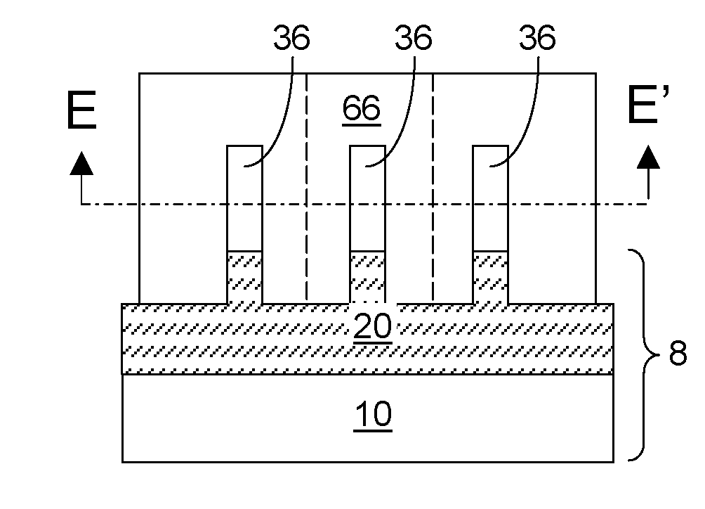
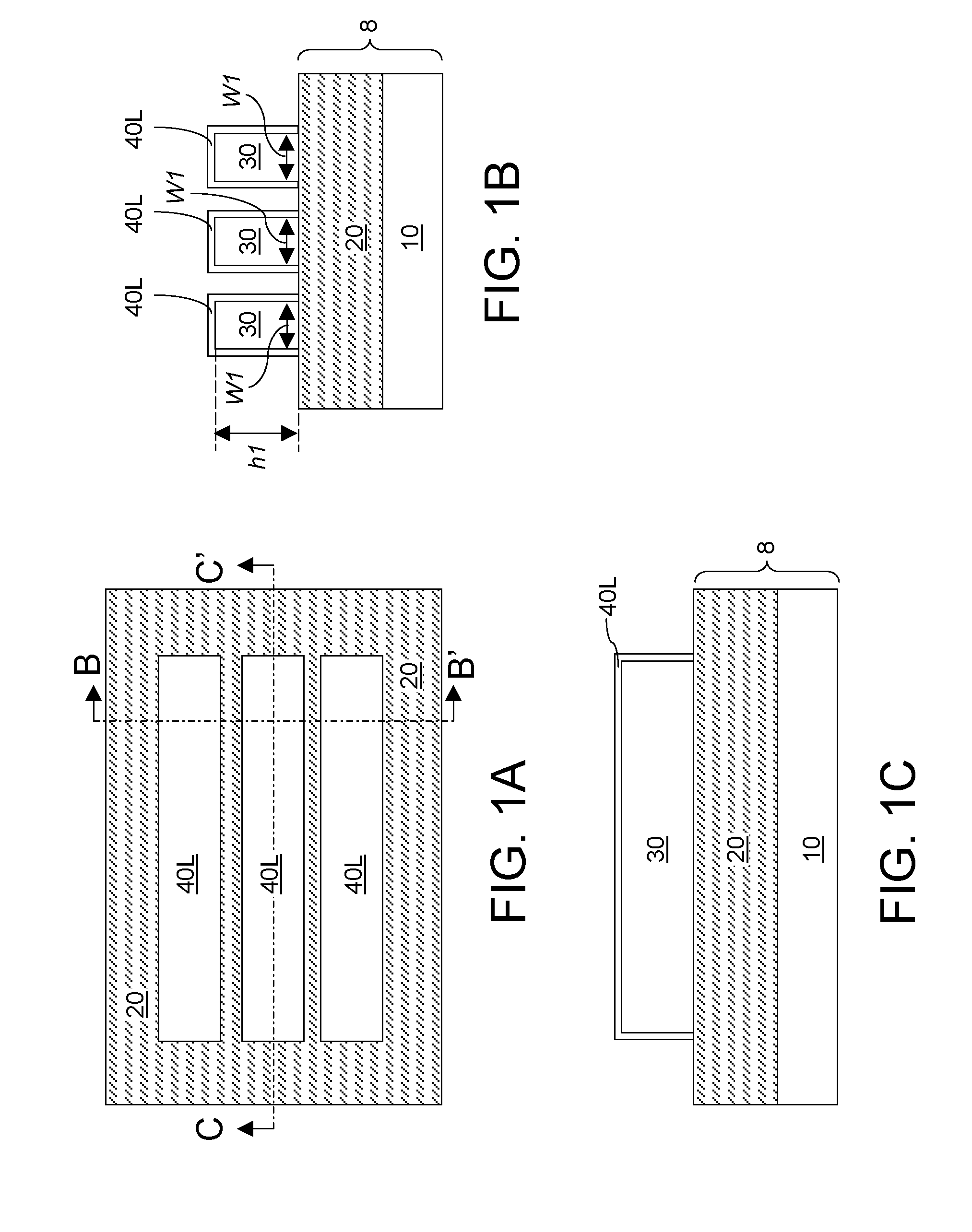
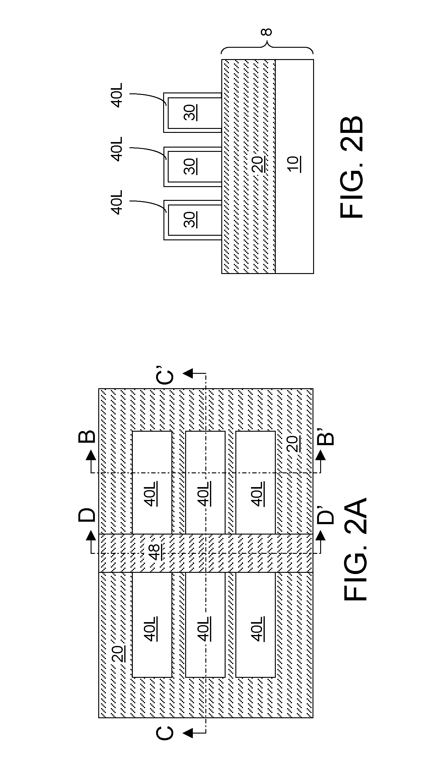
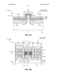
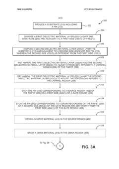
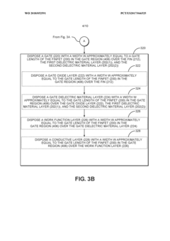
Finfet with longitudinal stress in a channel
PatentActiveUS20100038679A1
Innovation
- The method involves forming semiconductor fins on an insulator layer, etching the end portions to reduce their height and width, and growing lattice-mismatched semiconductor material epitaxially on these portions to apply longitudinal stress along the channel, using selective epitaxy to align the material with the fin, thereby enhancing device performance.

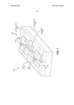
FIN field effect transistors (FETS) (finfets) employing dielectric material layers to apply stress to channel regions
PatentWO2018052591A1
Innovation
- Employing dielectric material layers on either side of the Fin to apply stress to the channel region, which provides consistent stress levels regardless of the FinFET area, unlike epitaxial layers or shallow trench isolation methods.
Thermal Management Strategies for AR FinFET Implementations
Thermal management represents a critical challenge in FinFET implementations for Augmented Reality (AR) devices. As AR applications demand increasingly powerful processing capabilities, the heat generated by FinFET-based chips has become a significant limiting factor affecting both performance and user experience. The compact form factor of AR headsets and glasses creates a particularly challenging thermal environment, with limited space for traditional cooling solutions.
Current thermal management strategies for AR FinFET implementations can be categorized into several approaches. At the semiconductor level, advanced materials with superior thermal conductivity are being integrated into FinFET designs. Silicon-on-insulator (SOI) substrates with optimized thermal properties have shown promising results in laboratory testing, reducing junction temperatures by up to 15% compared to conventional substrates.
Dynamic thermal management (DTM) techniques have emerged as essential software-hardware hybrid solutions. These systems continuously monitor temperature across the chip and dynamically adjust clock frequencies, voltage levels, and workload distribution to prevent thermal throttling while maintaining optimal performance. Machine learning algorithms are increasingly being deployed to predict thermal patterns and preemptively adjust processing parameters before critical temperature thresholds are reached.
Novel cooling technologies specifically designed for the spatial constraints of AR devices include ultra-thin vapor chambers and microfluidic cooling channels. These solutions can be integrated directly into the device frame, creating thermal pathways that efficiently dissipate heat away from the FinFET processors. Recent developments in phase-change materials (PCMs) embedded within AR device frames have demonstrated the ability to absorb thermal energy during peak processing loads and gradually release it during idle periods.
Architectural innovations in FinFET design are also addressing thermal challenges. Heterogeneous integration approaches that strategically position high-power processing elements away from heat-sensitive components have shown significant improvements in thermal management. 3D stacking technologies with integrated thermal vias provide vertical heat dissipation pathways, reducing hotspot formation.
Power management techniques specifically optimized for AR workloads complement these hardware solutions. Workload-aware power gating, which selectively deactivates unused portions of the chip based on application requirements, has demonstrated power reductions of up to 30% in AR rendering scenarios, with corresponding decreases in heat generation. Task scheduling algorithms that distribute computation to minimize thermal density have become essential components in AR operating systems.
The industry is increasingly adopting holistic thermal design approaches that consider the entire AR device ecosystem rather than focusing solely on the FinFET components. This includes thermally conscious placement of components, strategic use of the device's external surface for passive cooling, and adaptive performance profiles based on environmental conditions and usage patterns.
Power Efficiency Optimization for AR-Specific FinFET Designs
Power efficiency optimization represents a critical frontier in AR-specific FinFET designs, as augmented reality applications demand high computational performance within strict power constraints. Current AR devices face significant battery life limitations, typically operating for only 2-4 hours under normal usage conditions. This power constraint directly impacts user experience and limits the commercial viability of AR technologies in everyday applications.
FinFET architectures for AR must balance multiple competing requirements: high processing capability for real-time rendering, thermal management to ensure user comfort, and extended battery life to support practical usage scenarios. Recent advancements have focused on dynamic voltage and frequency scaling (DVFS) techniques specifically tailored for AR workloads, which can reduce power consumption by up to 35% compared to standard mobile processor implementations.
Multi-threshold voltage designs have emerged as particularly promising for AR applications, allowing different sections of the chip to operate at optimal power levels based on their specific functions. For example, display rendering components can utilize high-performance, higher-power transistors, while background processing elements can leverage lower-power variants, creating an overall more efficient system architecture.
Gate-all-around (GAA) FinFET variants show exceptional promise for AR implementations, demonstrating up to 40% improved power efficiency compared to traditional FinFET designs when handling mixed workloads typical in AR applications. These designs provide better electrostatic control and reduced leakage current, addressing key power consumption challenges in compact AR form factors.
Specialized cache hierarchies optimized for AR rendering pipelines represent another significant advancement. By implementing application-specific memory architectures that prioritize frequently accessed AR rendering data, recent designs have achieved 25-30% reductions in memory-related power consumption without compromising computational performance.
Thermal-aware power management systems have become increasingly sophisticated in AR-specific FinFET implementations. These systems dynamically adjust processing resources based on both computational demands and thermal conditions, preventing overheating while maximizing performance within available power envelopes. Recent implementations demonstrate the ability to maintain peak performance for 30% longer periods before thermal throttling becomes necessary.
Looking forward, heterogeneous integration approaches combining FinFET technology with specialized AR accelerators show tremendous potential for further power optimization. Early prototypes combining traditional FinFET cores with dedicated neural processing units and vision accelerators have demonstrated up to 60% improvements in performance-per-watt metrics for AR-specific computational tasks.
Unlock deeper insights with PatSnap Eureka Quick Research — get a full tech report to explore trends and direct your research. Try now!
Generate Your Research Report Instantly with AI Agent
Supercharge your innovation with PatSnap Eureka AI Agent Platform!