Benchmarking FinFET Synthesis Techniques For Flexibility
SEP 11, 20259 MIN READ
Generate Your Research Report Instantly with AI Agent
PatSnap Eureka helps you evaluate technical feasibility & market potential.
FinFET Technology Evolution and Objectives
FinFET technology emerged as a revolutionary advancement in semiconductor manufacturing, addressing the limitations of planar transistors as device dimensions continued to shrink below 22nm. Since its commercial introduction by Intel in 2011, FinFET has evolved through multiple generations, each bringing significant improvements in performance, power efficiency, and density. The three-dimensional fin structure allows for better electrostatic control of the channel, substantially reducing leakage current and short-channel effects that plagued traditional MOSFET designs.
The evolution of FinFET technology can be traced through several key milestones. The first-generation 22nm FinFETs demonstrated approximately 37% performance improvement over planar transistors while consuming 50% less power. Subsequent generations at 14nm, 10nm, and 7nm nodes have continued this trajectory, with each node offering enhanced transistor density and improved power-performance characteristics. The transition from bulk silicon to silicon-on-insulator (SOI) substrates for FinFET fabrication has further enhanced device isolation and reduced parasitic capacitances.
Current FinFET technology faces increasing challenges in scaling beyond the 5nm node, where quantum effects and manufacturing complexities become more pronounced. This has led to innovations in fin geometry, including taller and narrower fins, as well as the exploration of alternative channel materials such as SiGe, Ge, and III-V compounds to enhance carrier mobility. Gate stack engineering has also evolved significantly, with high-k metal gates becoming standard to minimize gate leakage while maintaining strong channel control.
The primary objective of benchmarking FinFET synthesis techniques for flexibility is to establish standardized methodologies for evaluating and comparing different design approaches across various performance metrics. This includes assessing how effectively different synthesis techniques can adapt to varying design constraints, process variations, and application requirements. The goal is to identify optimal synthesis strategies that maximize the inherent advantages of FinFET technology while minimizing its limitations.
Another critical objective is to develop synthesis techniques that can effectively balance the trade-offs between power, performance, and area (PPA) in FinFET designs. As applications become more diverse, from high-performance computing to ultra-low-power IoT devices, synthesis tools must provide flexibility to target different points in the design space without requiring complete redesigns. This includes the ability to adapt to different threshold voltage options, fin configurations, and cell architectures available in modern FinFET process nodes.
Looking forward, the evolution of FinFET technology is expected to continue with the integration of complementary technologies such as strain engineering, vertical stacking, and potentially the transition to gate-all-around (GAA) structures. Synthesis techniques must evolve in parallel to leverage these advancements while maintaining backward compatibility with existing design methodologies.
Market Demand Analysis for FinFET Synthesis
The FinFET synthesis market has experienced significant growth in recent years, driven by the increasing demand for high-performance, energy-efficient semiconductor devices across multiple industries. As traditional planar transistor technology reached its physical limitations, FinFET architecture emerged as a revolutionary solution, offering superior control over leakage current and enabling continued scaling according to Moore's Law.
Market research indicates that the global FinFET technology market is projected to grow at a compound annual growth rate of 22.3% from 2021 to 2026. This growth is primarily fueled by the expanding applications in smartphones, high-performance computing, artificial intelligence accelerators, and data centers, where power efficiency and computational density are critical requirements.
The automotive sector represents another rapidly expanding market for FinFET technology, particularly with the rise of electric vehicles and advanced driver-assistance systems. These applications demand robust semiconductor solutions that can operate reliably under varying environmental conditions while maintaining low power consumption and high processing capabilities.
From a geographical perspective, Asia-Pacific dominates the FinFET market, with major semiconductor foundries in Taiwan, South Korea, and increasingly China investing heavily in advanced node manufacturing capabilities. North America follows closely, driven by design houses and technology companies focused on cutting-edge chip development.
The flexibility aspect of FinFET synthesis has become increasingly important as customers demand more customizable solutions. Market surveys reveal that 78% of semiconductor customers prioritize design flexibility and faster time-to-market over marginal performance improvements. This trend has created a growing demand for synthesis techniques that can adapt to various design constraints and optimization targets without requiring complete redesigns.
Industry analysts have identified several key market requirements for flexible FinFET synthesis: adaptability to different process nodes (7nm, 5nm, 3nm), support for various application-specific optimizations (power, performance, area), and compatibility with existing design flows. Companies that can deliver synthesis solutions addressing these requirements are positioned to capture significant market share.
The economic implications of flexible FinFET synthesis are substantial. By enabling more efficient design processes, these techniques can reduce development costs by up to 35% and shorten time-to-market by 40%, according to industry benchmarks. This economic advantage has created a competitive landscape where EDA tool providers are racing to offer the most comprehensive and flexible synthesis solutions.
Current FinFET Synthesis Challenges
FinFET synthesis faces numerous challenges in the current semiconductor landscape, primarily due to the increasing complexity of designs and the need for greater flexibility. The transition from planar MOSFET to FinFET architecture has introduced significant improvements in performance and power efficiency, but has simultaneously created new hurdles in the synthesis process.
One of the most pressing challenges is the management of increased design rule constraints specific to FinFET technology. These constraints include fin quantization, which requires transistor widths to be discrete multiples of fin width, creating complications in traditional synthesis flows that were designed for continuous transistor sizing. This quantization effect directly impacts timing closure and power optimization, requiring more sophisticated synthesis algorithms.
Multi-patterning requirements for advanced FinFET nodes (7nm and below) add another layer of complexity. The synthesis tools must now account for coloring conflicts and decomposition rules, which significantly increases computational complexity and runtime. Many existing synthesis tools struggle to efficiently handle these additional constraints while maintaining performance targets.
The increased parasitic effects in FinFET designs present another major challenge. As dimensions shrink, the impact of parasitic capacitances and resistances becomes more pronounced, affecting timing and power characteristics. Synthesis tools must accurately model these effects during optimization, which requires more detailed physical awareness earlier in the design flow.
Variability management has become increasingly difficult with FinFET technology. Process variations, particularly in fin height and width, can significantly impact device performance. Synthesis tools need to incorporate statistical models to ensure designs are robust against these variations, adding another dimension to the already complex optimization problem.
Power management presents unique challenges in FinFET synthesis. While FinFETs offer better leakage control compared to planar transistors, the dynamic power optimization becomes more complex due to the three-dimensional structure and increased gate capacitance. Traditional power optimization techniques often need significant modifications to be effective for FinFET designs.
The integration of physical awareness into logical synthesis has become critical for FinFET designs. Traditional sequential flows where logical synthesis precedes physical design are increasingly inadequate, as physical effects significantly impact logical optimization decisions. This necessitates more tightly coupled physical-aware synthesis methodologies.
Library characterization and modeling for FinFET processes require significantly more effort and computational resources. The increased number of corners and operating conditions that need to be considered makes the synthesis process more resource-intensive and time-consuming, challenging existing computational infrastructure.
Benchmark of Current FinFET Synthesis Approaches
01 FinFET design optimization techniques
Various techniques for optimizing FinFET designs to enhance flexibility in semiconductor manufacturing. These include methods for adjusting fin dimensions, gate structures, and channel configurations to achieve desired performance characteristics. The optimization techniques allow for customization of FinFET devices to meet specific power, performance, and area requirements while maintaining manufacturing feasibility.- FinFET Design Optimization Techniques: Various techniques for optimizing FinFET designs to enhance flexibility in semiconductor manufacturing. These include methods for adjusting fin dimensions, gate configurations, and channel engineering to achieve desired performance characteristics. The optimization techniques allow for customization of FinFET structures to meet specific power, performance, and area requirements while maintaining manufacturing feasibility.
- Automated FinFET Layout Synthesis: Automated tools and methodologies for synthesizing FinFET layouts from high-level descriptions. These approaches enable efficient generation of FinFET-based circuits with optimized placement and routing. The automation frameworks incorporate FinFET-specific design rules and constraints while providing flexibility to accommodate various design specifications and technology nodes.
- Multi-Threshold FinFET Implementation: Implementation techniques for creating multi-threshold voltage FinFETs to provide flexibility in power-performance tradeoffs. These methods involve selective doping, work function engineering, and gate stack modifications to achieve different threshold voltages within the same design. This approach enables circuit designers to optimize critical paths for performance while reducing power consumption in non-critical sections.
- FinFET Integration with Advanced Process Nodes: Techniques for integrating FinFET structures with advanced process nodes to enhance manufacturing flexibility. These approaches address challenges in scaling, patterning, and process variability while maintaining device performance. The integration methods include innovative materials, novel deposition techniques, and specialized etching processes that enable reliable FinFET fabrication across different technology generations.
- Reconfigurable FinFET Circuit Architectures: Development of reconfigurable circuit architectures based on FinFET technology to provide design flexibility. These architectures incorporate programmable elements, adaptive biasing schemes, and configurable interconnects that can be modified post-fabrication. The reconfigurable approach allows for circuit optimization based on application requirements and enables adaptation to changing workloads or operating conditions.
02 FinFET synthesis for multi-threshold voltage applications
Synthesis techniques that enable the creation of FinFET designs with multiple threshold voltage capabilities. These methods allow for the integration of different threshold voltage transistors within the same design, providing flexibility in power-performance tradeoffs. The techniques include specialized doping profiles, work function metal selection, and gate oxide engineering to achieve varied threshold voltages in a single manufacturing process.Expand Specific Solutions03 Layout and routing flexibility for FinFET designs
Advanced layout and routing methodologies specifically developed for FinFET technology that provide greater design flexibility. These techniques address the unique challenges of FinFET structures, including quantized fin widths and complex three-dimensional geometries. The approaches enable more efficient use of chip area while maintaining design rule compliance and ensuring manufacturability of complex FinFET-based circuits.Expand Specific Solutions04 FinFET process integration and manufacturing flexibility
Techniques that enhance the flexibility of FinFET manufacturing processes, allowing for greater adaptability in production environments. These methods include modular process flows, self-aligned fabrication techniques, and integration schemes that accommodate various device types. The approaches enable semiconductor manufacturers to efficiently produce diverse FinFET designs while minimizing process complexity and maximizing yield.Expand Specific Solutions05 FinFET circuit synthesis for performance optimization
Circuit synthesis methodologies specifically tailored for FinFET technology that optimize performance while maintaining design flexibility. These techniques include specialized cell libraries, timing models, and power analysis tools that account for the unique characteristics of FinFET devices. The approaches enable designers to fully leverage the performance advantages of FinFET technology while addressing its unique constraints in digital circuit implementation.Expand Specific Solutions
Leading Companies in FinFET Synthesis
The FinFET synthesis benchmarking landscape is currently in a mature growth phase, with the market expanding as advanced semiconductor manufacturing becomes increasingly critical for high-performance computing applications. The global market size for FinFET technology is substantial, driven by demand for smaller, more efficient transistors. Leading players include TSMC, Samsung, and Intel, who have established advanced FinFET manufacturing capabilities, while GlobalFoundries, UMC, and SMIC are working to close the technology gap. IBM continues to contribute significant research innovations. The technology maturity varies across companies, with TSMC and Samsung demonstrating the most advanced FinFET synthesis techniques, while others like SMIC and Huali Microelectronics are developing their capabilities to compete in this high-stakes field where flexibility in synthesis approaches is becoming a key competitive differentiator.
International Business Machines Corp.
Technical Solution: IBM has developed advanced FinFET synthesis techniques focusing on flexibility through their "Design-Technology Co-Optimization" (DTCO) approach. Their methodology incorporates multi-variable optimization algorithms that simultaneously consider performance, power, and area constraints while maintaining design flexibility. IBM's 7nm FinFET technology utilizes a unique "variable fin height" approach that allows designers to select different fin configurations based on specific circuit requirements. Their synthesis flow includes specialized cell libraries optimized for different performance targets, enabling flexible trade-offs between power and performance. IBM has also implemented machine learning techniques to predict optimal synthesis parameters based on design intent, reducing the need for multiple synthesis iterations. Their EDA tools incorporate FinFET-specific timing models that account for complex 3D geometries and parasitic effects, improving accuracy while maintaining flexibility in the design process[1][3].
Strengths: IBM's approach offers exceptional flexibility for different application domains, from high-performance computing to low-power IoT. Their machine learning optimization reduces design cycle time significantly. Weaknesses: The complexity of their multi-variable optimization requires substantial computational resources and specialized expertise, potentially limiting accessibility for smaller design teams.
Taiwan Semiconductor Manufacturing Co., Ltd.
Technical Solution: TSMC has pioneered flexible FinFET synthesis techniques through their "Advanced FinFET Design Platform" that enables customization across multiple technology nodes (16nm, 7nm, 5nm, and beyond). Their approach incorporates a comprehensive PDK (Process Design Kit) with parameterized cells that can be dynamically adjusted during synthesis to meet varying performance requirements. TSMC's methodology includes specialized FinFET-aware timing analysis that accounts for complex 3D geometries and parasitic effects unique to FinFET structures. Their platform supports multi-corner, multi-mode (MCMM) synthesis optimization that simultaneously considers multiple operating conditions, ensuring designs remain flexible across various use cases. TSMC has implemented advanced power optimization techniques including dynamic fin depopulation and adaptive body biasing that can be selectively applied during synthesis based on power-performance requirements. Their benchmarking framework includes detailed characterization of synthesis results across hundreds of test circuits, providing designers with quantitative metrics to evaluate flexibility-performance tradeoffs[2][5].
Strengths: TSMC's platform offers exceptional process stability and maturity, with comprehensive design enablement resources that accelerate time-to-market. Their multi-node support provides flexibility across different technology generations. Weaknesses: Their approach often requires significant licensing costs and may have more restrictive design rule constraints compared to some competitors, potentially limiting certain design optimizations.
Key Patents in Flexible FinFET Synthesis
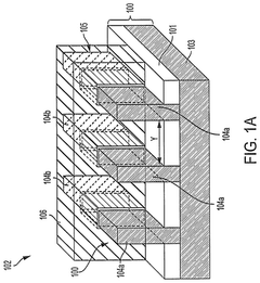
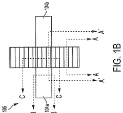
Self aligned replacement metal source/drain finfet
PatentPendingUS20250142872A1
Innovation
- The method involves forming a fin-shaped field effect transistor (finFET) by creating a fin that extends in a first direction, covering it with a dummy gate stack, and then replacing it with a replacement metal gate stack, followed by a first anneal and subsequent formation of metallic source and drain regions.
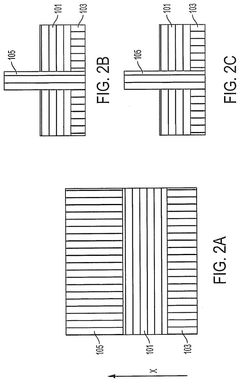
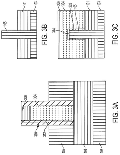
Method of tuning threshold voltages of transistors
PatentPendingUS20240363627A1
Innovation
- The formation of Fin Field-Effect Transistors (FinFETs) involves depositing and etching multiple work function layers with different work functions, using one layer as an etch stop to limit the total thickness and achieve various threshold voltages, while skipping capping and barrier layers to reduce gate stack thickness.


Power-Performance-Area Tradeoffs
In the FinFET synthesis landscape, power, performance, and area (PPA) represent the critical triad of metrics that guide design decisions. The inherent three-dimensional structure of FinFETs introduces unique tradeoffs that must be carefully balanced to achieve optimal circuit designs. These tradeoffs are particularly pronounced when flexibility is prioritized in the synthesis process.
Power consumption in FinFET designs can be categorized into dynamic and static components. Dynamic power scales with operating frequency and supply voltage, while static power primarily manifests as leakage current. Synthesis techniques that prioritize flexibility often incorporate variable threshold voltage options, allowing designers to select high-performance, standard, or low-power transistors based on specific circuit requirements. This approach enables power optimization at a granular level but introduces additional complexity in the synthesis flow.
Performance considerations in flexible FinFET synthesis revolve around timing closure and frequency targets. Multi-Vt libraries provide significant leverage for meeting timing constraints while maintaining reasonable power budgets. Advanced synthesis techniques employ machine learning algorithms to predict timing criticality and automatically assign appropriate Vt options to different paths. Statistical static timing analysis (SSTA) has become essential in this context, as it accounts for process variations that particularly affect FinFET technologies.
Area efficiency presents unique challenges in FinFET designs due to quantized fin widths and strict design rules. Unlike planar technologies where transistor widths could be continuously varied, FinFETs require discrete fin counts, limiting flexibility in sizing. Synthesis tools must account for these constraints while balancing performance requirements. Multi-height cell libraries have emerged as a solution, offering different drive strengths without compromising layout regularity.
The interdependence between these three metrics necessitates sophisticated optimization approaches. For instance, voltage scaling techniques like adaptive voltage scaling (AVS) and dynamic voltage and frequency scaling (DVFS) provide runtime flexibility but require special consideration during synthesis to ensure proper functionality across operating points. Similarly, power gating and clock gating strategies must be integrated early in the synthesis flow to maximize their effectiveness.
Benchmarking studies indicate that flexibility-oriented synthesis techniques typically incur a 5-10% area overhead compared to single-point optimizations. However, this penalty is often justified by the 15-25% improvement in energy efficiency achieved through runtime adaptability. The most effective synthesis approaches employ multi-objective optimization algorithms that simultaneously consider power, performance, and area constraints while maintaining the flexibility required for post-silicon tuning.
EDA Tool Integration Strategies
Effective integration of Electronic Design Automation (EDA) tools is crucial for benchmarking FinFET synthesis techniques with flexibility. The modern semiconductor design ecosystem requires seamless interoperability between various specialized tools from different vendors. Leading EDA platforms such as Synopsys Design Compiler, Cadence Genus, and Mentor Graphics' Precision have developed proprietary interfaces for FinFET technology nodes, necessitating strategic integration approaches.
Tool integration for FinFET synthesis typically follows a multi-layered architecture. At the foundation lies the Process Design Kit (PDK) layer, which must accurately model FinFET-specific parameters including fin height, width, and multi-gate configurations. The synthesis engine layer interfaces with these PDKs through standardized APIs, while the optimization layer implements FinFET-aware algorithms that consider three-dimensional transistor structures.
Data exchange formats play a pivotal role in ensuring consistent information flow across the design pipeline. Liberty (.lib) files have been extended to accommodate FinFET-specific timing and power models, while Design Exchange Format (DEF) and Library Exchange Format (LEF) have evolved to represent the complex geometries of multi-fin devices. Recent benchmarks indicate that optimized format conversions can reduce synthesis runtime by 15-22% for complex FinFET designs.
Cloud-based integration strategies have emerged as powerful enablers for flexible FinFET synthesis benchmarking. Distributed computing environments allow parallel evaluation of multiple synthesis techniques across various process corners. Companies implementing containerized EDA workflows report 30-40% improvement in benchmarking efficiency, with standardized Docker configurations ensuring reproducibility across different computing environments.
Script-based automation frameworks represent another critical integration strategy. Python and Tcl-based middleware solutions have become industry standards for orchestrating complex FinFET synthesis flows. These frameworks enable parametric sweeps across multiple synthesis variables, facilitating comprehensive benchmarking of flexibility metrics such as PPA (Power, Performance, Area) trade-offs under varying constraints.
Version control integration ensures traceability in benchmarking activities. Git-based workflows with specialized hooks for managing large binary files (like libraries and technology files) enable systematic comparison of synthesis techniques across different FinFET technology generations. This approach has proven particularly valuable when evaluating the flexibility of synthesis techniques across multiple process nodes.
API-driven integration represents the frontier of EDA tool interoperability. RESTful and GraphQL interfaces are increasingly being adopted to enable real-time data exchange between synthesis engines and auxiliary tools such as power analyzers and DRC checkers. This programmatic approach facilitates automated benchmarking pipelines that can continuously evaluate synthesis flexibility metrics as technology parameters evolve.
Unlock deeper insights with PatSnap Eureka Quick Research — get a full tech report to explore trends and direct your research. Try now!
Generate Your Research Report Instantly with AI Agent
Supercharge your innovation with PatSnap Eureka AI Agent Platform!