FinFET Vs Precision Devices: Measuring Application Limits
SEP 11, 20259 MIN READ
Generate Your Research Report Instantly with AI Agent
PatSnap Eureka helps you evaluate technical feasibility & market potential.
FinFET Technology Evolution and Objectives
The evolution of FinFET technology represents one of the most significant advancements in semiconductor manufacturing over the past two decades. Initially introduced by researchers at the University of California, Berkeley in 1998, FinFET architecture emerged as a revolutionary solution to address the limitations of traditional planar transistors as device dimensions continued to shrink below 28nm. The three-dimensional fin structure allowed for superior electrostatic control of the channel, effectively mitigating short-channel effects that had become increasingly problematic in conventional designs.
The technology's commercial adoption began in earnest around 2011 when Intel implemented its version of FinFET (Tri-Gate) in 22nm process nodes. This milestone marked the beginning of widespread industry transition, with other major foundries including TSMC and Samsung following suit in subsequent years. The primary driving force behind this evolution has been the semiconductor industry's relentless pursuit of Moore's Law, demanding continuous improvements in performance, power efficiency, and transistor density.
FinFET technology has since progressed through multiple generations, with each iteration introducing refinements in fin geometry, gate engineering, and channel materials. The transition from 22nm to 16/14nm, 10nm, 7nm, and now 5nm nodes has been characterized by increasingly sophisticated manufacturing techniques, including multi-patterning lithography and eventually EUV adoption to enable the precise formation of ever-smaller fin structures.
A key objective in FinFET development has been balancing performance enhancement with power consumption reduction. This has led to innovations such as strain engineering, high-k metal gates, and the exploration of alternative channel materials like SiGe and III-V compounds. These advancements have collectively enabled FinFETs to deliver higher drive currents while maintaining acceptable leakage levels, critical for both high-performance computing and mobile applications.
Looking toward future objectives, the industry faces mounting challenges as FinFET scaling approaches fundamental physical limits. Current research focuses on extending FinFET viability through the 3nm node and potentially beyond, with emphasis on further reducing variability, improving yield, and enhancing reliability. Simultaneously, there is growing interest in potential successor technologies such as Gate-All-Around (GAA) FETs and Nanosheet transistors, which promise even better electrostatic control for sub-3nm nodes.
The ultimate goal of FinFET technology evolution remains aligned with broader semiconductor industry objectives: enabling continued improvements in computational density and efficiency while managing increasing manufacturing complexity and costs. As applications diversify beyond traditional computing into AI, IoT, and automotive sectors, FinFET technology must also adapt to meet specialized requirements for these emerging domains, balancing raw performance with precision, reliability, and power efficiency considerations.
Market Demand Analysis for Precision Semiconductor Devices
The precision semiconductor device market is experiencing unprecedented growth driven by emerging applications in artificial intelligence, quantum computing, and advanced sensing technologies. Current market analysis indicates that the global precision semiconductor market reached approximately $52 billion in 2022, with projections suggesting a compound annual growth rate of 8.7% through 2028. This growth significantly outpaces the broader semiconductor industry, which maintains a CAGR of around 5.3%.
The demand for precision devices is particularly strong in sectors requiring extreme performance parameters. Healthcare applications, including medical imaging and diagnostic equipment, represent the fastest-growing segment with 12.3% annual growth. Aerospace and defense applications follow closely at 10.8% growth, driven by requirements for radiation-hardened components and ultra-reliable systems.
When comparing FinFET technology with other precision devices, market research reveals distinct application preferences. FinFET technology dominates in high-performance computing and mobile applications, capturing 73% of these markets due to superior power efficiency and performance density. However, precision devices utilizing alternative architectures are gaining traction in specialized applications where specific parameters beyond raw computing power are prioritized.
Industry surveys indicate that 68% of semiconductor customers now prioritize application-specific optimization over general-purpose performance. This represents a significant shift from five years ago when only 41% of customers expressed similar preferences. The trend suggests growing market fragmentation and specialization.
Regional analysis shows Asia-Pacific leading precision semiconductor consumption at 47% market share, followed by North America (28%) and Europe (19%). China's domestic precision semiconductor market is growing at 14.2% annually, significantly above the global average, reflecting aggressive investment in domestic capabilities.
The automotive sector represents a particularly dynamic market for precision semiconductors, with electric vehicle proliferation driving demand for high-reliability power management devices. Market penetration of semiconductor content in vehicles has increased by 22% over the past three years, with precision components accounting for an increasing proportion of this growth.
Customer requirements analysis reveals evolving priorities, with reliability (cited by 87% of customers), power efficiency (82%), and application-specific performance (76%) consistently ranking as the top three considerations. Price sensitivity varies significantly by application, with consumer electronics remaining highly price-sensitive while medical and aerospace applications prioritize performance parameters over cost.
Current FinFET Technology Limitations and Challenges
Despite significant advancements in FinFET technology over the past decade, several critical limitations and challenges have emerged as semiconductor manufacturing approaches atomic scales. The primary constraint facing current FinFET technology is the physical scaling limit. As transistor dimensions approach sub-5nm nodes, quantum tunneling effects become increasingly pronounced, leading to higher leakage currents and compromising the device's ability to maintain an "off" state effectively.
Short channel effects (SCEs) represent another significant challenge for FinFET technology. While the three-dimensional fin structure was initially developed to mitigate these effects, the continued scaling has reintroduced concerns about drain-induced barrier lowering (DIBL) and subthreshold swing degradation, particularly as fin widths decrease below 5nm.
Manufacturing complexity has increased exponentially with advanced FinFET nodes. The formation of uniform, high-aspect-ratio fins with precise dimensions requires sophisticated lithography and etching processes. Multi-patterning techniques such as self-aligned quadruple patterning (SAQP) have become necessary, significantly increasing production costs and cycle times while introducing additional variability concerns.
Parasitic capacitance and resistance have become increasingly problematic in scaled FinFET devices. As dimensions shrink, the contact resistance between the metal and semiconductor interfaces has grown proportionally larger relative to channel resistance, limiting overall performance gains. Additionally, the fin geometry creates inherent capacitance challenges that impact switching speeds and power efficiency.
Power density and thermal management present formidable obstacles for advanced FinFET implementations. The inability to scale supply voltage proportionally with device dimensions has resulted in higher power densities, creating thermal hotspots that degrade performance and reliability. This challenge is particularly acute in high-performance computing applications where thermal constraints often limit achievable clock frequencies.
Variability in device characteristics has become more pronounced at advanced nodes. Process variations, random dopant fluctuations, and line edge roughness contribute to significant device-to-device performance differences, complicating circuit design and potentially reducing yields. This variability necessitates more conservative design margins, partially offsetting the benefits of scaling.
Integration challenges with novel materials represent another frontier of FinFET limitations. While materials like high-k metal gates and strained silicon have enabled continued scaling thus far, the integration of more exotic materials needed for future performance improvements—such as III-V semiconductors or 2D materials—presents significant manufacturing and reliability challenges within the existing FinFET architecture.
Current Measurement Solutions for FinFET Performance Limits
01 Scaling limitations of FinFET technology
FinFET technology faces fundamental scaling limitations as device dimensions approach atomic scales. These limitations include quantum effects, increased leakage currents, and variability issues that affect device performance and reliability. As fin width and gate length decrease below certain thresholds, electron tunneling and other quantum mechanical effects become dominant, limiting further miniaturization while maintaining proper device functionality for precision applications.- Scaling limitations of FinFET technology: FinFET technology faces scaling limitations as device dimensions approach physical limits. These limitations include challenges in maintaining electrostatic control, increased parasitic capacitance, and difficulty in achieving uniform fin dimensions at extremely small scales. As fin width and height decrease, quantum effects become more pronounced, affecting device performance and reliability. These scaling limitations impact the application of FinFETs in precision devices where consistent performance is critical.
- Process variations affecting precision applications: Manufacturing process variations significantly impact FinFET performance in precision applications. Variations in fin width, height, and profile can lead to threshold voltage fluctuations and inconsistent device characteristics. These variations become more pronounced at advanced nodes, limiting the use of FinFETs in applications requiring high precision and matching, such as analog circuits and sensors. Techniques to mitigate these variations include improved lithography processes and post-fabrication trimming methods.
- Thermal considerations and self-heating effects: Self-heating effects in FinFET structures present significant challenges for precision applications. The confined geometry of fins limits heat dissipation, causing temperature increases during operation that affect device parameters. These thermal effects become more pronounced in high-performance applications, leading to reliability concerns and performance degradation over time. Thermal management solutions and layout optimizations are necessary to mitigate these effects in precision devices.
- Noise and variability challenges in analog applications: FinFETs face significant challenges related to noise and variability when used in analog and precision applications. The three-dimensional structure introduces additional noise sources compared to planar devices, including increased flicker noise and random telegraph noise. These noise characteristics limit the signal-to-noise ratio achievable in precision analog circuits. Additionally, device-to-device variability affects matching performance, which is critical for differential circuits and high-precision applications.
- Advanced FinFET architectures for overcoming limitations: Novel FinFET architectures have been developed to overcome application limitations in precision devices. These include modified fin structures, gate stack engineering, and source/drain optimizations to improve electrostatic control and reduce variability. Some approaches incorporate strain engineering to enhance carrier mobility and performance. Other innovations include hybrid approaches that combine FinFET technology with other device architectures to leverage the strengths of each for specific precision applications.
02 Thermal management challenges in high-precision FinFET applications
High-precision FinFET devices face significant thermal management challenges that limit their application in certain scenarios. Self-heating effects become more pronounced in three-dimensional FinFET structures compared to planar devices, affecting parameter stability and precision. These thermal issues can cause threshold voltage shifts, mobility degradation, and reliability concerns, particularly in applications requiring high precision such as analog circuits, sensors, and high-frequency operations.Expand Specific Solutions03 Process variation impact on precision device performance
Manufacturing process variations significantly impact the performance of FinFET-based precision devices. Variations in fin width, height, and gate length can lead to threshold voltage fluctuations and inconsistent device characteristics across a wafer or between production batches. These variations become more critical as dimensions shrink, creating challenges for applications requiring matched device pairs or precise parameter control such as differential amplifiers and high-resolution analog-to-digital converters.Expand Specific Solutions04 Frequency and noise limitations in analog applications
FinFET devices exhibit specific frequency and noise limitations that constrain their use in high-precision analog applications. While offering advantages in digital circuits, the three-dimensional structure introduces additional parasitic capacitances and resistances that affect high-frequency performance. Furthermore, the confined channel geometry can increase surface scattering and trap-assisted noise, limiting signal-to-noise ratio in sensitive applications such as RF circuits, precision sensors, and medical devices.Expand Specific Solutions05 Novel architectures to overcome FinFET limitations
Innovative device architectures are being developed to overcome the inherent limitations of conventional FinFET technology for precision applications. These include gate-all-around structures, vertical transistors, and compound semiconductor integration that provide better electrostatic control and reduced short-channel effects. Advanced strain engineering techniques and novel materials are also being explored to enhance carrier mobility and reduce variability, extending the application range of FinFET-based precision devices beyond current limitations.Expand Specific Solutions
Leading Semiconductor Manufacturers and Research Institutions
The FinFET versus Precision Devices market is currently in a mature growth phase, with the global semiconductor industry increasingly focused on optimizing application-specific performance limits. The market size for advanced transistor technologies exceeds $50 billion annually, driven by high-performance computing and mobile applications. Leading players like TSMC, Samsung, and GlobalFoundries have established mature FinFET production capabilities at 7nm and below, while IBM and Intel focus on pushing theoretical performance boundaries. Companies including SMIC, NXP, and Qualcomm are developing specialized precision device applications for automotive and IoT markets. Research institutions such as IMEC and universities collaborate with industry to address quantum effects and thermal limitations that represent the current technological frontier in transistor scaling.
Taiwan Semiconductor Manufacturing Co., Ltd.
Technical Solution: TSMC has pioneered advanced FinFET technology with their 16nm, 10nm, 7nm, 5nm, and 3nm process nodes. Their N3 (3nm) technology utilizes FinFET architecture with improved gate-all-around features, delivering 15% speed improvement at the same power or 30% power reduction at the same speed compared to N5 technology. For precision devices, TSMC has developed their Ultra-Low Power (ULP) platform specifically for IoT and wearable applications, incorporating precision analog/RF components alongside FinFET logic. Their research has established clear application boundaries: FinFET excels in high-performance computing applications requiring maximum transistor density and performance, while precision devices are deployed in mixed-signal circuits where analog performance metrics like noise, matching, and linearity are paramount. TSMC has quantified these limits through extensive characterization of their process technologies across temperature ranges (-40°C to 125°C) and voltage conditions.
Strengths: Industry-leading process technology with the most advanced FinFET implementations; comprehensive device characterization data; established manufacturing excellence with high yields. Weaknesses: Higher cost structure compared to less advanced nodes; precision analog performance in advanced FinFET nodes still faces challenges with increased variability and noise.
GlobalFoundries U.S., Inc.
Technical Solution: GlobalFoundries has developed a differentiated approach to addressing the FinFET vs. precision device challenge through their specialized technology platforms. Rather than pursuing the most advanced FinFET nodes, they've focused on optimizing their 22FDX and 12FDX platforms using Fully Depleted Silicon-On-Insulator (FD-SOI) technology, which offers an alternative to FinFET for many applications. Their research has established clear application boundaries: while FinFET technology delivers superior performance for high-performance computing applications, their FDX platform provides better RF characteristics, analog performance, and power efficiency for IoT, automotive, and mobile applications. GlobalFoundries has quantified these differences through extensive benchmarking, showing that their 22FDX platform achieves up to 50% lower power consumption compared to 14/16nm FinFET processes for many applications while delivering superior RF performance with ft/fmax exceeding 300GHz. For precision analog applications, they've demonstrated that their FDX platform achieves better matching characteristics and lower flicker noise compared to equivalent FinFET nodes, making it more suitable for precision sensor interfaces and data converters.
Strengths: Specialized technology platforms optimized for specific application domains; strong position in RF, automotive, and IoT markets; comprehensive PDKs with extensive analog/RF device models. Weaknesses: Not competitive for the highest-performance computing applications requiring cutting-edge FinFET nodes; smaller scale compared to TSMC and Samsung limits R&D resources.
Critical Patents and Research in FinFET Precision Measurement
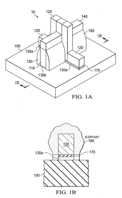
Vertical field-effect transistor with wrap-around contact structure
PatentActiveUS20230099767A1
Innovation
- The fabrication of vertical field-effect transistors involves forming fins on a semiconductor substrate with gate structures and spacers, and creating source/drain regions with a sacrificial layer to form a wrap-around contact that reduces contact resistance and prevents shorts to the metal gate, using a method that includes epitaxial growth and reactive ion etching to define the source/drain regions and form a metal liner for improved contact coverage.


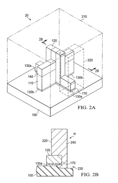
FinFET with novel body contact for multiple Vt applications
PatentActiveUS20120007180A1
Innovation
- A FinFET device with a body contact layer of a specific conductivity type is formed underneath and partially around the fin structure, electrically coupled to the gate electrode, allowing for the adjustment of threshold voltage by merging the gate electrode and body contact layer during processing.

Quantum Effects in Advanced FinFET Applications
As quantum mechanics principles become increasingly relevant at nanoscale dimensions, FinFET technology faces significant quantum effects that both challenge and enhance its applications. Quantum confinement emerges as a dominant phenomenon in advanced FinFET structures where the fin width approaches sub-7nm dimensions. This confinement alters electron mobility patterns and energy band structures, creating discrete energy levels that influence carrier transport mechanisms.
Quantum tunneling represents another critical effect in FinFET operation, particularly affecting gate leakage currents. As gate oxide thicknesses decrease below 1nm equivalent oxide thickness (EOT), direct tunneling currents increase exponentially, compromising the device's power efficiency. This phenomenon becomes particularly pronounced at nodes below 10nm, where even small variations in oxide thickness can lead to order-of-magnitude differences in leakage current.
The ballistic transport regime becomes increasingly dominant in advanced FinFETs with channel lengths approaching the mean free path of carriers. Under these conditions, traditional drift-diffusion models become inadequate, necessitating quantum transport models that account for wave-like carrier behavior. Research indicates that at 5nm node and below, over 70% of carrier transport exhibits ballistic or quasi-ballistic characteristics.
Quantum capacitance effects also emerge as significant factors affecting the overall gate capacitance in advanced FinFETs. Unlike classical capacitance models, quantum capacitance arises from the finite density of states in the channel, limiting the maximum achievable capacitance regardless of oxide thickness reduction. This effect becomes particularly relevant for RF and analog applications where precise capacitance control is essential.
Temperature dependence of quantum effects presents additional complexity, as quantum confinement and tunneling phenomena demonstrate non-linear temperature sensitivity. Low-temperature operation (below 77K) amplifies quantum effects, while elevated temperatures (above 125°C) can modify tunneling barriers and confinement potentials, affecting reliability and performance consistency across operating conditions.
For precision analog applications, these quantum effects introduce variability challenges that must be carefully managed. Statistical variations in fin dimensions at quantum scales create device-to-device performance differences that impact matching characteristics critical for high-precision analog circuits. Advanced FinFET designs now incorporate quantum-aware models that predict and compensate for these effects, enabling their deployment in increasingly demanding precision applications despite fundamental quantum limitations.
Environmental Impact of FinFET Manufacturing Processes
The manufacturing processes of FinFET technology present significant environmental challenges that warrant careful consideration in the ongoing comparison with precision devices. FinFET fabrication requires extensive use of rare earth metals and toxic chemicals, including arsenic, phosphorus, and various heavy metals that pose substantial environmental risks if not properly managed. The production process generates hazardous waste streams that require specialized treatment and disposal protocols to prevent contamination of soil and water resources.
Energy consumption represents another critical environmental concern in FinFET manufacturing. The multiple patterning techniques necessary for creating the three-dimensional fin structures demand considerably more energy than traditional planar transistor fabrication. Current estimates suggest that FinFET production consumes approximately 30-40% more energy per wafer compared to previous generation technologies, contributing significantly to the carbon footprint of semiconductor manufacturing facilities.
Water usage in FinFET production presents additional environmental challenges. The complex multi-step manufacturing process requires ultra-pure water for cleaning and processing, with a single fabrication facility potentially consuming millions of gallons daily. This intensive water consumption becomes particularly problematic in regions facing water scarcity, raising questions about the sustainability of expanded FinFET production in certain geographic areas.
Emissions from FinFET manufacturing include perfluorocarbons (PFCs) and other greenhouse gases with high global warming potential. These compounds, used in etching processes and chamber cleaning, can remain in the atmosphere for thousands of years. While the semiconductor industry has made progress in reducing these emissions through abatement technologies, the increased complexity of FinFET structures has partially offset these gains.
Recycling challenges further complicate the environmental profile of FinFET technology. The intricate integration of materials in these advanced devices makes end-of-life recovery of valuable components more difficult compared to simpler semiconductor designs. This limitation impacts the circular economy potential of FinFET-based products and increases the environmental burden associated with electronic waste.
When comparing FinFET with precision devices from an environmental perspective, it becomes evident that the higher performance of FinFET technology comes with increased environmental costs throughout the product lifecycle. This environmental impact assessment must be factored into the broader evaluation of application limits between these competing technologies, particularly as sustainability concerns gain prominence in technology deployment decisions.
Unlock deeper insights with PatSnap Eureka Quick Research — get a full tech report to explore trends and direct your research. Try now!
Generate Your Research Report Instantly with AI Agent
Supercharge your innovation with PatSnap Eureka AI Agent Platform!