FinFET Functions For Circuit Density Maximization
SEP 11, 20259 MIN READ
Generate Your Research Report Instantly with AI Agent
PatSnap Eureka helps you evaluate technical feasibility & market potential.
FinFET Evolution and Density Optimization Goals
The evolution of FinFET technology represents one of the most significant advancements in semiconductor manufacturing over the past two decades. Since its commercial introduction by Intel in 2011 with their 22nm process node, FinFET has become the dominant transistor architecture for advanced integrated circuits. This three-dimensional structure emerged as a solution to the physical limitations of planar transistors, particularly short-channel effects that became increasingly problematic below the 28nm node.
The technological trajectory of FinFET has been characterized by continuous refinement in fin geometry, with height-to-width ratios steadily increasing to enhance current drive capability while minimizing leakage. Early implementations featured relatively thick fins with limited height, whereas modern FinFETs utilize taller, narrower fins that maximize effective channel width per unit area. This evolution directly correlates with circuit density improvements, as more efficient transistors enable smaller cell designs.
Density optimization goals for FinFET technology have consistently focused on several key parameters: reducing the fin pitch, optimizing gate length, minimizing source/drain contact areas, and improving metal routing efficiency. The industry has progressed from initial fin pitches of approximately 60nm to current leading-edge processes achieving sub-20nm fin pitches, representing a threefold improvement in potential transistor density.
Another critical aspect of FinFET evolution has been the transition from double-gate to tri-gate and eventually gate-all-around configurations, each providing enhanced electrostatic control and allowing for further dimensional scaling. These architectural improvements have enabled continued adherence to density scaling targets that approximate historical Moore's Law projections, albeit at increasing technical complexity and cost.
The ultimate goal of FinFET density optimization extends beyond simple transistor count increases. Modern objectives include optimizing power-performance-area (PPA) metrics holistically, as power constraints have become equally important as density in many applications. This has led to innovations in circuit design techniques specifically tailored to FinFET characteristics, such as multi-Vt implementations, self-aligned double patterning, and advanced strain engineering.
Looking forward, the industry is approaching fundamental physical limits of the traditional FinFET architecture, with sub-5nm nodes requiring novel approaches. The transition pathway toward nanosheet/nanowire structures represents the logical evolution of FinFET principles, maintaining the goal of maximizing circuit density while addressing the increasing challenges of power dissipation and manufacturing variability at extreme dimensions.
Market Demand for High-Density Integrated Circuits
The global market for high-density integrated circuits continues to experience robust growth, driven primarily by the increasing demand for advanced computing capabilities across multiple sectors. The semiconductor industry has witnessed a compound annual growth rate of approximately 6% over the past five years, with the high-density IC segment growing even faster at nearly 9% annually. This accelerated growth reflects the critical importance of circuit density maximization in modern electronic systems.
Consumer electronics remains the largest market segment demanding high-density integrated circuits, accounting for roughly 40% of the total market share. Smartphones, tablets, and wearable devices require increasingly powerful processors in ever-smaller form factors, making FinFET technology particularly valuable in this space. The average smartphone now contains over 50 integrated circuits, with the main application processor utilizing advanced FinFET technology to deliver maximum performance within strict power and space constraints.
Data centers and cloud computing infrastructure represent the fastest-growing segment for high-density ICs, with demand increasing at nearly 15% annually. The exponential growth in data processing requirements, coupled with energy efficiency concerns, has positioned FinFET-based processors as essential components in modern server architectures. Major cloud service providers are consistently upgrading their hardware to incorporate the latest high-density circuit technologies to maintain competitive advantages in performance and operational costs.
The automotive sector has emerged as a significant new market for high-density integrated circuits, particularly with the advancement of electric vehicles and autonomous driving technologies. Advanced driver assistance systems (ADAS) and infotainment systems require substantial computing power in space-constrained environments, creating ideal applications for FinFET-based solutions. Industry analysts project that semiconductor content in premium vehicles will increase by over 30% in the next five years, with high-density ICs representing a substantial portion of this growth.
Industrial IoT applications are creating additional demand vectors for high-density integrated circuits. Smart manufacturing systems, industrial automation, and connected infrastructure all require edge computing capabilities that balance performance with power efficiency. The industrial sector is expected to deploy over 15 billion connected devices by 2025, many requiring advanced processing capabilities that only high-density circuit technologies can provide.
Geographic market distribution shows Asia-Pacific leading consumption at 60% of the global market, followed by North America at 25% and Europe at 12%. China's ambitious semiconductor self-sufficiency initiatives have further accelerated regional demand for advanced manufacturing capabilities, including those related to FinFET technology and high-density circuit design methodologies.
Current FinFET Technology Limitations and Challenges
Despite significant advancements in FinFET technology, several critical limitations and challenges persist that impede further circuit density maximization. The fundamental physical constraints of current FinFET architectures have become increasingly apparent as dimensions approach sub-5nm nodes. Short-channel effects (SCEs), while better controlled than in planar transistors, still manifest as gate length decreases below 10nm, resulting in increased leakage current and degraded subthreshold swing characteristics.
Quantum mechanical effects present another significant barrier, with electron tunneling becoming pronounced at extremely small dimensions. This phenomenon leads to unpredictable device behavior and compromises the reliability of integrated circuits. Additionally, the three-dimensional nature of FinFETs introduces complex fabrication challenges, particularly in achieving uniform fin dimensions and consistent doping profiles across billions of transistors.
Process variability has emerged as a critical concern, with minor variations in fin width, height, and gate length significantly impacting threshold voltage and drive current. This variability directly affects circuit performance and yield rates, creating substantial challenges for high-volume manufacturing. Furthermore, self-heating effects become more pronounced in densely packed FinFET structures, where thermal dissipation paths are constrained, potentially leading to reliability issues and performance degradation over time.
The parasitic capacitance between adjacent fins and gates increases as device dimensions shrink, negatively impacting switching speed and power consumption. Current FinFET designs also face limitations in contact resistance optimization, with smaller contact areas leading to higher resistance and consequent performance penalties. These parasitic elements become increasingly dominant factors in overall circuit performance as scaling continues.
Integration challenges with back-end-of-line (BEOL) processes represent another significant hurdle. As transistor density increases, the metal interconnect scaling becomes problematic, with resistance-capacitance (RC) delays in interconnects often overshadowing transistor switching delays. This interconnect bottleneck threatens to undermine the benefits gained from transistor scaling.
From a manufacturing perspective, extreme ultraviolet (EUV) lithography adoption remains challenging due to cost and technical complexities, while multi-patterning techniques introduce additional process steps and potential for defects. The economic viability of continued FinFET scaling is also questionable, with exponentially increasing fabrication costs not always justified by proportional performance improvements.
These multifaceted challenges collectively suggest that conventional FinFET technology may be approaching its practical scaling limits, necessitating exploration of alternative architectures or complementary technologies to continue the trajectory of circuit density maximization in future semiconductor generations.
Current Approaches to FinFET Circuit Density Enhancement
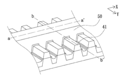
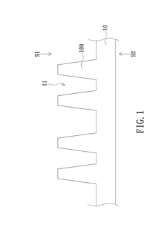
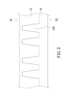
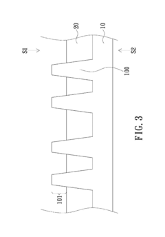
01 FinFET structure design for increased circuit density
Various structural designs of FinFETs can significantly increase circuit density. These include optimizing fin height, width, and spacing, as well as implementing multi-fin structures. Advanced gate designs and reduced channel lengths also contribute to higher density integration while maintaining performance characteristics. These structural optimizations allow for more transistors to be packed into smaller areas without compromising electrical properties.- FinFET structure optimization for increased circuit density: Optimizing the structure of FinFETs can significantly increase circuit density. This includes designing multi-gate transistors with reduced fin pitch, implementing vertical fins, and utilizing 3D stacking techniques. These structural optimizations allow for more transistors to be packed into a smaller area, thereby increasing the overall circuit density while maintaining or improving performance characteristics.
- Advanced layout techniques for FinFET circuit density: Advanced layout techniques specifically designed for FinFET technology can enhance circuit density. These techniques include optimized cell libraries, track height reduction, and innovative placement algorithms. By carefully arranging FinFET components and minimizing the space between them, designers can achieve higher circuit density without compromising electrical performance or manufacturability.
- Integration of FinFETs with other semiconductor technologies: Integrating FinFETs with other semiconductor technologies can lead to improved circuit density. This includes combining FinFETs with planar transistors, memory elements, or passive components in a single chip. Such heterogeneous integration allows for optimized use of silicon area, with each technology being used where it provides the most benefit in terms of performance and area efficiency.
- Novel materials and processes for FinFET density enhancement: The use of novel materials and fabrication processes can enhance FinFET circuit density. This includes implementing high-k dielectric materials, metal gates, strain engineering, and advanced lithography techniques. These innovations allow for smaller feature sizes, reduced parasitic capacitances, and improved electrical characteristics, all contributing to higher circuit density without sacrificing performance.
- Power and thermal management for high-density FinFET circuits: Effective power and thermal management techniques are essential for high-density FinFET circuits. These include dynamic voltage and frequency scaling, power gating, and innovative cooling solutions. By addressing the increased power density and heat generation that comes with higher circuit density, these approaches ensure reliable operation of densely packed FinFET circuits while maintaining performance and extending device lifetime.
02 Multi-gate and 3D integration techniques
Multi-gate architectures and 3D integration techniques enable significant improvements in FinFET circuit density. By stacking transistors vertically and implementing double or triple gate configurations, chip area utilization is maximized. These approaches allow for more efficient use of silicon real estate while maintaining or improving electrical performance. Advanced 3D integration methods also facilitate better interconnection between transistor layers, reducing overall circuit footprint.Expand Specific Solutions03 Novel materials and fabrication processes
Incorporating novel materials and advanced fabrication processes can enhance FinFET circuit density. High-k dielectric materials, metal gates, and strain engineering techniques improve transistor performance while allowing for smaller dimensions. Innovative lithography and etching methods enable more precise pattern definition and tighter spacing between components. These material and process innovations collectively contribute to higher integration density without sacrificing device reliability.Expand Specific Solutions04 Layout optimization and cell design techniques
Optimized layout strategies and cell design techniques are crucial for maximizing FinFET circuit density. Advanced placement algorithms, track height reduction, and efficient routing methodologies minimize wasted space. Standard cell libraries specifically designed for FinFET technology can achieve higher packing density through careful consideration of fin quantization and power rail placement. These design approaches enable more efficient utilization of available chip area.Expand Specific Solutions05 Integration with complementary technologies
Integrating FinFETs with complementary technologies enhances overall circuit density. Combining FinFETs with advanced interconnect schemes, embedded memory technologies, and system-on-chip architectures creates more compact integrated circuits. Hybrid approaches that leverage the strengths of different transistor types in appropriate circuit blocks optimize both performance and density. These integration strategies enable higher functionality within constrained die areas.Expand Specific Solutions
Leading Semiconductor Manufacturers and IP Providers
The FinFET technology market for circuit density maximization is currently in a mature growth phase, with an estimated global market size exceeding $50 billion. Leading players include Taiwan Semiconductor Manufacturing Co. (TSMC), which dominates with advanced 5nm and 3nm FinFET processes, followed by Samsung and Intel. GLOBALFOUNDRIES and Semiconductor Manufacturing International Corporation (SMIC) are competing in the mid-tier segment, while Applied Materials and IBM provide critical equipment and research support. The technology maturity varies significantly, with TSMC and Samsung achieving commercial production at advanced nodes, while SMIC faces development constraints due to trade restrictions. Companies like Apple and NVIDIA are driving demand as key customers requiring cutting-edge FinFET technology for their high-performance computing applications.
Taiwan Semiconductor Manufacturing Co., Ltd.
Technical Solution: TSMC has pioneered advanced FinFET technology with their leading-edge process nodes. Their N5 and N3 FinFET technologies implement multi-fin structures with reduced fin pitch and height optimization to maximize circuit density. TSMC employs a unique "track height" reduction approach in their standard cell libraries, allowing for more compact circuit layouts. Their FinFET designs feature specialized source/drain epitaxial growth techniques that minimize parasitic resistance while maintaining tight spacing between transistors. TSMC has also developed innovative local interconnect schemes specifically for FinFET structures that reduce the metal layer requirements and improve vertical integration density. Their contact-over-active-gate (COAG) technology enables direct contacts to transistor gates without additional spacing requirements, significantly improving circuit density in logic applications.
Strengths: Industry-leading process technology with proven high-volume manufacturing capability; excellent electrostatic control with minimal leakage current; superior scaling roadmap with clear path to sub-3nm nodes. Weaknesses: Higher manufacturing complexity requiring sophisticated lithography tools; increased process variability at extreme scaling nodes; higher production costs compared to planar transistor technologies.
International Business Machines Corp.
Technical Solution: IBM has been a pioneer in FinFET research and development, with fundamental contributions to the technology's evolution. Their approach to circuit density maximization focuses on unique gate formation techniques that enable tighter packing of transistors. IBM's FinFET technology incorporates specialized self-aligned double patterning methods that achieve sub-lithographic feature sizes without requiring extreme ultraviolet lithography. Their designs feature a proprietary strain engineering approach that maintains carrier mobility enhancement even at reduced fin dimensions. IBM has developed innovative work function metal integration schemes that allow for optimized threshold voltages while minimizing gate-to-gate spacing requirements. Additionally, their research has demonstrated novel dielectric materials for spacer regions that provide improved electrical isolation with reduced physical dimensions, directly contributing to higher achievable circuit densities.
Strengths: Strong fundamental research capabilities with extensive patent portfolio; innovative materials science approach to transistor design; excellent academic and research partnerships. Weaknesses: Limited commercial manufacturing capacity; technology often licensed to manufacturing partners rather than produced internally; focus has shifted more toward quantum computing and other emerging technologies.
Key Patents in FinFET Density Maximization Techniques
Finfets with long gate length at high density
PatentInactiveUS20060154426A1
Innovation
- The method involves forming FinFET fins at an angle relative to the gate conductors and increasing fin density using multiple sidewall image transfer processing to pattern the silicon layer, allowing longer fins without increasing the array size by doubling the fin density.


Fin field effect transistor device and fabrication method thereof
PatentActiveUS20160163837A1
Innovation
- A method for fabricating a FinFET device involving the formation of a substrate with a fin structure, an oxide layer, shallow trench isolation, spacers, and an epitaxial fin structure, where the gate structure is perpendicular to the epitaxial fin, and the epitaxial fin can be made of germanium with varying compositions, allowing for improved electrical control and efficiency.
Power-Performance-Area Tradeoffs in Advanced FinFET Designs
The optimization of FinFET technology represents a critical balancing act between power consumption, performance capabilities, and area utilization. Advanced FinFET designs must carefully navigate these three competing factors to achieve optimal circuit density while maintaining functional integrity. This tradeoff triangle forms the foundation of modern semiconductor development strategies.
Power consumption in FinFET structures can be categorized into static and dynamic components. Static power primarily stems from leakage currents, which have been significantly reduced through innovations like high-k metal gates and optimized fin geometries. Dynamic power, associated with switching activities, scales with operating frequency and supply voltage. Recent advancements in FinFET design have enabled voltage scaling below 0.7V while maintaining performance targets, representing a substantial improvement over planar transistor technologies.
Performance metrics for FinFETs are predominantly measured through switching speed and drive current capabilities. The three-dimensional fin structure provides superior channel control, resulting in enhanced carrier mobility and reduced short-channel effects. Multi-fin configurations can be implemented to increase drive current, though this approach directly impacts area utilization. Industry benchmarks indicate that 7nm FinFET nodes achieve approximately 30-40% performance improvement over 10nm nodes, while simultaneously reducing power consumption by 25-35%.
Area efficiency remains perhaps the most challenging aspect of FinFET optimization. While fin pitch scaling continues to drive density improvements, physical limitations are becoming increasingly apparent. Innovative approaches such as self-aligned double patterning (SADP) and self-aligned quadruple patterning (SAQP) have enabled fin pitches below 30nm. Additionally, track height reduction in standard cells has emerged as a complementary strategy for area optimization, with leading foundries implementing 6-track and even 5-track cell libraries.
The interdependence of these three factors necessitates sophisticated design methodologies. For instance, reducing supply voltage to minimize power consumption typically requires wider transistors to maintain performance targets, directly impacting area efficiency. Similarly, aggressive fin pitch scaling for area optimization may introduce variability issues that compromise performance consistency or increase leakage power.
Recent research indicates that machine learning-assisted design space exploration is emerging as a promising approach for navigating these complex tradeoffs. By rapidly evaluating thousands of potential design configurations, AI algorithms can identify non-intuitive optimization points that human designers might overlook. This represents a paradigm shift in how power-performance-area tradeoffs are managed in advanced FinFET designs.
Thermal Management Solutions for Ultra-Dense FinFET Circuits
As FinFET technology continues to advance toward higher circuit densities, thermal management has emerged as a critical challenge that can significantly impact performance, reliability, and longevity of integrated circuits. The increasing power density in ultra-dense FinFET designs creates concentrated heat zones that conventional cooling methods struggle to address effectively.
Current thermal management solutions for ultra-dense FinFET circuits employ multi-layered approaches. At the device level, advanced materials with superior thermal conductivity properties are being integrated into the fabrication process. Silicon-on-insulator (SOI) substrates with modified thermal characteristics and thermally conductive dielectrics help facilitate better heat dissipation from the active regions of FinFETs.
On-chip thermal sensors and dynamic thermal management (DTM) systems represent another crucial advancement. These systems continuously monitor temperature distributions across the die and implement real-time adjustments to workload distribution, clock frequencies, and supply voltages to prevent thermal runaway conditions. Machine learning algorithms are increasingly being employed to predict thermal patterns and preemptively adjust operating parameters before critical temperatures are reached.
Microfluidic cooling channels integrated directly into the chip package represent one of the most promising recent innovations. These microscale channels allow coolant to flow in close proximity to hotspots, dramatically improving heat transfer efficiency compared to traditional heat sink approaches. Research indicates that such systems can handle heat fluxes exceeding 500 W/cm², which is essential for next-generation FinFET densities.
3D integration techniques are being leveraged not only for performance gains but also for thermal optimization. Through-silicon vias (TSVs) filled with thermally conductive materials serve dual purposes as electrical interconnects and thermal conduits. Strategic placement of these thermal TSVs near high-activity circuit blocks significantly reduces junction temperatures.
Advanced packaging solutions incorporating phase-change materials (PCMs) help manage transient thermal loads. These materials absorb heat during high-activity periods by changing phase, then release it gradually during lower-activity periods, effectively dampening temperature fluctuations that can stress FinFET structures and accelerate aging mechanisms.
Industry-academic collaborations are exploring more exotic approaches, including diamond-based heat spreaders, graphene thermal interfaces, and even chip-scale thermoelectric cooling elements. While these technologies remain primarily in research phases, they show promise for addressing the extreme thermal challenges projected for sub-3nm FinFET nodes where circuit densities may exceed 100 million transistors per square millimeter.
Unlock deeper insights with PatSnap Eureka Quick Research — get a full tech report to explore trends and direct your research. Try now!
Generate Your Research Report Instantly with AI Agent
Supercharge your innovation with PatSnap Eureka AI Agent Platform!