Application of Neuromorphic Chips in Electronic Devices
OCT 9, 202510 MIN READ
Generate Your Research Report Instantly with AI Agent
Patsnap Eureka helps you evaluate technical feasibility & market potential.
Neuromorphic Computing Background and Objectives
Neuromorphic computing represents a paradigm shift in electronic system design, drawing inspiration from the structure and function of the human brain. This approach emerged in the late 1980s when Carver Mead introduced the concept of using analog circuits to mimic neurobiological architectures. Over the past three decades, neuromorphic computing has evolved from theoretical frameworks to practical implementations, with significant acceleration in development occurring in the last decade due to advancements in materials science, fabrication techniques, and artificial intelligence algorithms.
The fundamental principle behind neuromorphic chips lies in their ability to process information in a parallel, event-driven manner similar to biological neural networks. Unlike traditional von Neumann architecture that separates processing and memory units, neuromorphic systems integrate computation and memory, enabling more efficient information processing for specific tasks. This architectural difference represents a critical evolutionary step in computing technology, potentially addressing the limitations of conventional computing paradigms, particularly for applications requiring real-time processing of sensory data.
Current technological trends indicate a convergence of neuromorphic computing with edge computing and Internet of Things (IoT) applications. This convergence is driven by the increasing demand for intelligent electronic devices capable of processing complex sensory information with minimal power consumption. The neuromorphic approach offers promising solutions for implementing artificial intelligence directly on devices without relying heavily on cloud infrastructure, thereby reducing latency and enhancing privacy.
The primary technical objectives for neuromorphic chips in electronic devices include achieving ultra-low power consumption while maintaining high computational efficiency for neural network operations. Research aims to develop chips capable of learning and adapting to new information in real-time, similar to biological systems. Additionally, there is a focus on creating scalable architectures that can be integrated into various electronic devices, from smartphones and wearables to autonomous vehicles and industrial sensors.
Another critical objective involves bridging the gap between neuromorphic hardware and existing software ecosystems. This includes developing programming models, compilers, and tools that allow developers to leverage neuromorphic capabilities without requiring expertise in neuromorphic engineering. The standardization of interfaces and protocols for neuromorphic systems represents a significant challenge that must be addressed to facilitate widespread adoption.
Looking forward, the field is moving toward the development of hybrid systems that combine traditional digital processing with neuromorphic elements, creating more versatile and efficient computing platforms. These systems aim to harness the strengths of both approaches, potentially revolutionizing how electronic devices process information and interact with the physical world.
Market Demand Analysis for Brain-Inspired Computing
The global market for brain-inspired computing technologies is experiencing unprecedented growth, driven by increasing demands for more efficient and intelligent electronic devices. Current projections indicate that the neuromorphic computing market will reach approximately $8.9 billion by 2025, with a compound annual growth rate of 86.4% from 2019 to 2025. This remarkable growth trajectory reflects the expanding applications of neuromorphic chips across various industries.
The primary market demand stems from artificial intelligence applications requiring real-time processing capabilities with minimal power consumption. Traditional von Neumann architecture-based processors face significant limitations in meeting these requirements, creating a substantial market gap that neuromorphic chips are positioned to fill. Industries such as autonomous vehicles, robotics, and advanced IoT devices are actively seeking solutions that can process sensory data with the efficiency and adaptability of biological neural systems.
Healthcare represents another significant market segment, with growing demand for neuromorphic solutions in medical imaging, patient monitoring systems, and brain-computer interfaces. The ability of these chips to process complex patterns in biological data while consuming minimal power makes them particularly valuable for portable and implantable medical devices. Market research indicates that healthcare applications alone could constitute 23% of the total neuromorphic chip market by 2027.
Consumer electronics manufacturers are increasingly exploring neuromorphic computing to enhance user experiences through more intuitive and responsive devices. Smartphones, wearables, and smart home systems benefit from the ability to process sensory information locally with minimal latency and power consumption. This edge computing capability addresses growing consumer concerns about privacy and reduces dependence on cloud connectivity.
The defense and aerospace sectors represent premium market segments with specific demands for neuromorphic technologies. These industries require systems capable of autonomous decision-making in challenging environments with strict power and weight constraints. Market analysis shows defense applications currently account for approximately 18% of neuromorphic chip implementations, with projected growth to 22% by 2026.
Geographically, North America currently leads the market with approximately 42% share, followed by Europe at 28% and Asia-Pacific at 24%. However, the Asia-Pacific region is expected to demonstrate the highest growth rate over the next five years, driven by substantial investments in AI technologies by countries like China, Japan, and South Korea.
A significant market driver is the growing emphasis on sustainable computing solutions. With data centers currently consuming approximately 1% of global electricity, the energy efficiency of neuromorphic chips—often requiring only 1/1000th the power of conventional processors for certain tasks—represents a compelling value proposition for environmentally conscious enterprises and governments implementing green technology initiatives.
Current State and Technical Challenges in Neuromorphic Chips
Neuromorphic computing has witnessed significant advancements in recent years, with major research institutions and technology companies investing heavily in this field. Current neuromorphic chips, such as IBM's TrueNorth, Intel's Loihi, and BrainChip's Akida, represent the state-of-the-art in hardware implementations that mimic neural processing. These chips demonstrate remarkable capabilities in pattern recognition, sensory processing, and adaptive learning while consuming significantly less power than traditional computing architectures.
Despite these achievements, neuromorphic computing faces several critical technical challenges. The foremost challenge lies in scaling these systems to match the complexity of biological neural networks. The human brain contains approximately 86 billion neurons with trillions of synaptic connections, while current neuromorphic chips typically incorporate only millions of artificial neurons. This scaling gap limits the complexity of problems these chips can effectively address.
Material science presents another significant hurdle. Current CMOS technology, while adaptable for neuromorphic designs, imposes limitations on energy efficiency and integration density. Emerging materials such as memristors, phase-change memory, and spintronic devices show promise for more efficient synaptic implementations but face challenges in manufacturing consistency, reliability, and integration with existing semiconductor processes.
Programming paradigms for neuromorphic systems remain underdeveloped compared to conventional computing. Traditional algorithmic approaches do not translate efficiently to neuromorphic architectures, necessitating new programming models that can effectively harness the parallel, event-driven nature of these systems. This creates a significant barrier to adoption for developers accustomed to conventional computing paradigms.
The lack of standardization across neuromorphic platforms further complicates development efforts. Different neuromorphic chips employ varying architectures, learning rules, and communication protocols, making it difficult to develop applications that can run across multiple platforms. This fragmentation slows ecosystem growth and limits commercial adoption.
Energy efficiency, while superior to traditional computing for certain tasks, still falls short of biological systems. The human brain operates at approximately 20 watts, whereas scaled neuromorphic systems would require substantially more power. Bridging this efficiency gap remains a critical challenge for practical applications, particularly in mobile and edge computing scenarios.
Geographically, neuromorphic research shows concentration in North America, Europe, and East Asia. The United States leads with significant investments from both government agencies like DARPA and major corporations. Europe has established strong research clusters through initiatives like the Human Brain Project, while China, Japan, and South Korea are rapidly expanding their neuromorphic research capabilities through national strategic initiatives.
Current Neuromorphic Integration Solutions for Electronic Devices
01 Neuromorphic architecture design
Neuromorphic chips are designed with architectures that mimic the structure and functionality of the human brain. These designs incorporate neural networks, synaptic connections, and processing elements that enable parallel processing and efficient computation. The architecture typically includes arrays of artificial neurons and synapses that can process information in a manner similar to biological neural systems, allowing for more efficient handling of complex cognitive tasks and pattern recognition.- Neuromorphic architecture design: Neuromorphic chips are designed to mimic the structure and functionality of the human brain, featuring neural networks with interconnected artificial neurons and synapses. These architectures enable parallel processing, event-driven computation, and spike-based information processing. The designs incorporate specialized circuits that emulate neurobiological functions, allowing for efficient pattern recognition and cognitive tasks while consuming significantly less power than traditional computing architectures.
- Memristor-based neuromorphic systems: Memristors serve as key components in neuromorphic chips by emulating synaptic behavior through their variable resistance states. These non-volatile memory devices can store and process information simultaneously, enabling efficient implementation of neural networks in hardware. Memristor-based neuromorphic systems offer advantages in power efficiency, density, and learning capabilities, making them suitable for edge computing applications and artificial intelligence tasks that require adaptive learning and pattern recognition.
- Spiking neural networks implementation: Spiking neural networks (SNNs) represent a biologically inspired approach to neuromorphic computing where information is processed using discrete spikes or events rather than continuous signals. These implementations use specialized hardware to efficiently process temporal information and enable unsupervised learning. SNN-based neuromorphic chips can perform complex pattern recognition tasks with significantly lower power consumption compared to traditional deep learning approaches, making them suitable for real-time processing in resource-constrained environments.
- On-chip learning and adaptation mechanisms: Neuromorphic chips incorporate on-chip learning capabilities that allow them to adapt to new data and environments without requiring external training. These systems implement various plasticity mechanisms inspired by biological learning processes such as spike-timing-dependent plasticity (STDP) and homeostatic plasticity. The on-chip learning capabilities enable continuous adaptation, fault tolerance, and improved performance in dynamic environments, making these chips suitable for autonomous systems and edge AI applications.
- Integration with conventional computing systems: Neuromorphic chips are designed to interface with traditional computing architectures, creating hybrid systems that leverage the strengths of both paradigms. These integration approaches include specialized interfaces, co-processors, and software frameworks that enable seamless communication between neuromorphic and conventional components. The hybrid systems can accelerate specific AI workloads while maintaining compatibility with existing software ecosystems, facilitating the adoption of neuromorphic computing in various applications including robotics, IoT devices, and data centers.
02 Memristor-based neuromorphic computing
Memristors are used in neuromorphic chips to simulate synaptic behavior, enabling efficient implementation of neural networks in hardware. These devices can change their resistance based on the history of current flow, mimicking the plasticity of biological synapses. Memristor-based neuromorphic systems offer advantages in terms of power efficiency, density, and the ability to perform both memory and computing functions in the same device, making them ideal for edge computing applications and artificial intelligence tasks.Expand Specific Solutions03 Spiking neural networks implementation
Spiking neural networks (SNNs) are implemented in neuromorphic chips to more accurately replicate the behavior of biological neurons. Unlike traditional artificial neural networks, SNNs process information using discrete spikes or events, similar to how neurons in the brain communicate. This approach enables more energy-efficient computation and better temporal information processing. Neuromorphic chips designed for SNNs incorporate specialized circuits for spike generation, propagation, and learning mechanisms such as spike-timing-dependent plasticity.Expand Specific Solutions04 On-chip learning and adaptation
Neuromorphic chips incorporate on-chip learning capabilities that allow them to adapt and improve performance over time. These systems can modify their internal parameters based on input data, enabling continuous learning without requiring external training. Various learning algorithms are implemented directly in hardware, including unsupervised, supervised, and reinforcement learning approaches. This capability makes neuromorphic chips particularly suitable for applications requiring adaptation to changing environments or tasks, such as autonomous systems and real-time data processing.Expand Specific Solutions05 Energy-efficient neuromorphic computing
Neuromorphic chips are designed with a focus on energy efficiency, significantly reducing power consumption compared to traditional computing architectures. These chips achieve energy efficiency through various techniques, including event-driven processing, where computation occurs only when necessary, and low-power analog or mixed-signal circuits that operate at lower voltages. The brain-inspired design allows for efficient parallel processing of information with minimal energy requirements, making these chips ideal for battery-powered devices, edge computing, and applications where power constraints are critical.Expand Specific Solutions
Key Industry Players in Neuromorphic Chip Development
The neuromorphic chip market is experiencing rapid growth in the electronic devices sector, currently in its early commercialization phase with expanding applications across edge computing, IoT, and AI-enabled devices. Market size is projected to reach significant scale by 2030, driven by increasing demand for energy-efficient AI processing. While technical maturity varies, industry leaders like IBM, Samsung, and Syntiant are advancing commercial deployment, with IBM's TrueNorth and Samsung's neuromorphic architectures showing promising results. Emerging players including Polyn Technology and Beijing Lingxi are accelerating innovation, while research institutions such as KAIST, Tsinghua University, and Peking University are contributing fundamental breakthroughs in neuromorphic computing architectures and materials.
International Business Machines Corp.
Technical Solution: IBM's TrueNorth neuromorphic chip architecture represents one of the most advanced implementations in the field, featuring a million programmable neurons and 256 million synapses organized into 4,096 neurosynaptic cores. The chip mimics the brain's structure with event-driven computation, consuming only 70mW of power while delivering 46 billion synaptic operations per second per watt. IBM has demonstrated TrueNorth's application in real-time video analysis, pattern recognition, and sensory processing tasks. The company has further evolved this technology with their next-generation neuromorphic systems that incorporate advanced materials for analog computing capabilities, enabling more efficient processing of neural network operations directly in memory. IBM's neuromorphic solutions have been integrated into edge computing devices for applications requiring real-time sensory processing with minimal power consumption, such as autonomous drones, IoT sensors, and mobile devices requiring advanced AI capabilities without cloud connectivity.
Strengths: Extremely low power consumption (70mW) compared to traditional processors; highly scalable architecture; proven performance in real-world applications; mature development ecosystem. Weaknesses: Programming complexity requires specialized knowledge; limited compatibility with conventional computing paradigms; higher initial implementation costs compared to traditional processors.
Hewlett Packard Enterprise Development LP
Technical Solution: HPE's neuromorphic computing approach centers around their memristor-based technology and the development of their "dot product engine" architecture. Their solution leverages crossbar arrays of memristive devices that can perform matrix operations in memory, eliminating the energy-intensive data movement between memory and processing units that plagues conventional computing architectures. HPE's neuromorphic chips utilize analog computing principles where memristors store neural network weights as conductance values, enabling highly efficient vector-matrix multiplications essential for neural network operations. This architecture has demonstrated up to 100x improvement in energy efficiency for AI workloads compared to conventional digital implementations. HPE has applied this technology to create accelerators for edge computing devices that can perform complex pattern recognition tasks with minimal power consumption. Their neuromorphic solutions have been integrated into prototype systems for image recognition, natural language processing, and anomaly detection in IoT environments, with particular success in applications requiring real-time processing of sensory data under strict power constraints.
Strengths: Memristor-based architecture offers exceptional energy efficiency; analog computing approach provides high computational density; mature fabrication processes leverage existing semiconductor infrastructure; strong integration with HPE's broader edge computing ecosystem. Weaknesses: Analog computing faces precision and variability challenges; technology still transitioning from research to commercial deployment; requires specialized programming models different from mainstream AI frameworks.
Core Neuromorphic Architecture and Algorithm Innovations
Neuromorphic device
PatentActiveUS20170193359A1
Innovation
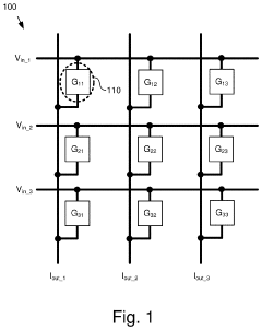
- A neuromorphic device design featuring a stack structure with reactive metal layers and an oxygen diffusion-retarding layer, where the thickness of the oxygen diffusion-retarding layer varies along the direction, allowing for controlled formation and disappearance of dielectric oxide layers, ensuring gradual and symmetric conductivity changes.
Hardware Accelerated Discretized Neural Network
PatentActiveUS20210334338A1
Innovation
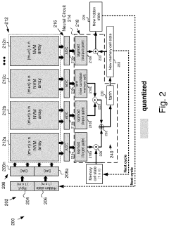
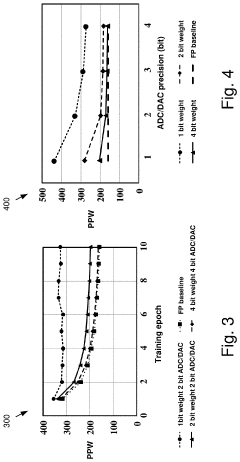
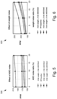
- A quantized neural network architecture that converts digital input and hidden state signals into analog form, processes them using non-volatile memory weight arrays for vector matrix multiplication, and then converts back to digital, with bit-widths reduced to 4 bits or less, utilizing DACs and ADCs to maintain performance comparable to 32-bit implementations.
Energy Efficiency Considerations for Neuromorphic Systems
Energy efficiency represents a critical consideration in the development and deployment of neuromorphic computing systems. Unlike traditional von Neumann architectures that consume significant power during data transfer between memory and processing units, neuromorphic chips mimic the brain's efficiency by integrating memory and computation. This fundamental architectural difference enables neuromorphic systems to achieve remarkable energy savings, with some implementations demonstrating 100-1000x improvement in energy efficiency compared to conventional computing approaches for specific tasks.
The power consumption profile of neuromorphic systems stems from their event-driven processing nature. Unlike conventional processors that continuously consume power regardless of computational load, neuromorphic chips activate only when processing spikes or events, significantly reducing idle power consumption. This characteristic makes them particularly suitable for edge computing applications in battery-powered electronic devices where energy constraints are paramount.
Material selection and fabrication techniques play crucial roles in determining the energy efficiency of neuromorphic hardware. Recent advancements in memristive technologies, phase-change materials, and spintronic devices have enabled the development of synaptic elements that require minimal energy for state changes. These innovations allow neuromorphic systems to perform complex pattern recognition tasks while consuming only milliwatts or even microwatts of power.
Scaling considerations present both opportunities and challenges for neuromorphic energy efficiency. While increasing the number of neurons and synapses enhances computational capabilities, it also introduces additional energy requirements. Researchers are exploring hierarchical architectures and sparse coding techniques to maintain efficiency at scale, drawing inspiration from the brain's ability to process information with minimal energy despite its vast neural network.
The energy advantages of neuromorphic systems become particularly evident in always-on sensing applications. For instance, neuromorphic vision sensors can perform continuous visual monitoring while consuming orders of magnitude less power than conventional camera systems. This efficiency stems from their ability to process only changes in the visual field rather than capturing and processing complete frames at fixed intervals.
Temperature management represents another important aspect of neuromorphic energy considerations. Lower power consumption naturally results in reduced heat generation, potentially eliminating the need for active cooling systems in many applications. This characteristic further enhances the overall energy profile of neuromorphic solutions when deployed in resource-constrained environments.
Standardization Efforts in Neuromorphic Hardware Interfaces
The standardization of neuromorphic hardware interfaces represents a critical frontier in advancing the widespread adoption of neuromorphic computing technologies. Currently, the field faces significant fragmentation, with various research institutions and companies developing proprietary interfaces and protocols for their neuromorphic chips. This lack of standardization creates substantial barriers to interoperability, hindering the integration of neuromorphic components into mainstream electronic devices.
Several industry consortia have emerged to address this challenge. The Neuromorphic Engineering Community (NEC) has been working since 2019 to establish common communication protocols between neuromorphic processors and conventional computing systems. Their efforts have resulted in the preliminary Neuromorphic Interface Protocol (NIP) specification, which defines standard methods for event-based data transmission and spike encoding schemes.
In parallel, the IEEE P2788 Working Group is developing standards specifically for neuromorphic device interfaces, focusing on creating uniform APIs that abstract hardware-specific details. This initiative aims to enable software developers to create applications that can run across different neuromorphic platforms without extensive modification, similar to how CUDA provides a standard interface for GPU computing.
The European Neuromorphic Computing Initiative (ENCI) has proposed the Common Neuromorphic Interface Framework (CNIF), which emphasizes standardized event representation formats and timing protocols. This framework has gained traction among European research institutions and has been implemented in several experimental platforms, demonstrating improved interoperability between different neuromorphic systems.
Major industry players like Intel, IBM, and Qualcomm have also begun collaborating on the Neuromorphic Hardware Interface Consortium (NHIC), recognizing that standardization is essential for market growth. Their joint specification focuses on power management interfaces, thermal considerations, and integration with conventional computing architectures—practical aspects critical for commercial electronic device applications.
Challenges to standardization efforts include balancing flexibility with specificity, accommodating the diverse architectural approaches in neuromorphic computing, and ensuring standards don't prematurely constrain innovation in this rapidly evolving field. The tension between established semiconductor companies favoring compatibility with existing systems and neuromorphic startups pushing for more radical approaches has also slowed consensus building.
Despite these challenges, progress in standardization is accelerating, with the first widely accepted interface standards expected within the next two years. These emerging standards will likely focus initially on spike encoding formats, event timing protocols, and basic power management interfaces, with more comprehensive standards evolving as the technology matures.
Unlock deeper insights with Patsnap Eureka Quick Research — get a full tech report to explore trends and direct your research. Try now!
Generate Your Research Report Instantly with AI Agent
Supercharge your innovation with Patsnap Eureka AI Agent Platform!