Comparison of Neuromorphic Chips vs Conventional Semiconductors
OCT 9, 20259 MIN READ
Generate Your Research Report Instantly with AI Agent
Patsnap Eureka helps you evaluate technical feasibility & market potential.
Neuromorphic Computing Evolution and Objectives
Neuromorphic computing represents a paradigm shift in computational architecture, drawing inspiration from the structure and function of the human brain. The evolution of this field began in the late 1980s when Carver Mead first introduced the concept of using electronic analog circuits to mimic neuro-biological architectures. This marked the beginning of a journey to create computing systems that could process information in ways similar to biological neural networks, offering potential advantages in efficiency and capability for certain types of computational tasks.
The development trajectory of neuromorphic computing has been characterized by several distinct phases. The initial phase focused on theoretical foundations and basic circuit designs. The second phase, spanning the 1990s to early 2000s, saw the emergence of small-scale neuromorphic systems primarily in academic research settings. The current phase, beginning around 2010, has witnessed significant acceleration with major investments from both industry and government entities, resulting in more sophisticated and practical implementations.
Key technological milestones include the development of silicon neurons, spike-based communication protocols, and learning algorithms that can be implemented in hardware. Projects such as IBM's TrueNorth, Intel's Loihi, and BrainScaleS from the Human Brain Project represent significant advances in scaling neuromorphic architectures to contain millions of neurons and billions of synapses.
The fundamental objective of neuromorphic computing is to overcome the limitations of conventional von Neumann architecture, particularly in terms of energy efficiency and the ability to process unstructured data. While conventional semiconductors excel at precise, sequential calculations, they face inherent bottlenecks when dealing with parallel, adaptive tasks that characterize many real-world problems.
Current research aims to develop neuromorphic systems that can achieve brain-like efficiency—the human brain operates on approximately 20 watts of power while performing complex cognitive tasks that would require megawatts of power in conventional computing systems. Additionally, these systems target capabilities such as online learning, fault tolerance, and contextual adaptation that are challenging for traditional computing paradigms.
The evolution of neuromorphic computing is increasingly driven by applications in artificial intelligence, particularly in areas requiring real-time processing of sensory data, pattern recognition, and decision-making under uncertainty. As conventional semiconductor scaling approaches physical limits, neuromorphic architectures offer a promising alternative path for continued advancement in computing capabilities, especially for edge computing applications where power efficiency is paramount.
Market Demand Analysis for Brain-Inspired Computing
The brain-inspired computing market is experiencing unprecedented growth, driven by the increasing demand for efficient processing of complex AI workloads. Current market research indicates that neuromorphic computing is projected to grow at a compound annual growth rate of 89% through 2025, reaching a market value of approximately 8 billion dollars by 2028. This exponential growth reflects the urgent need for computing architectures that can handle the massive computational requirements of modern AI applications while maintaining energy efficiency.
The primary market drivers for neuromorphic chips stem from limitations in conventional semiconductor technology. Traditional von Neumann architectures face significant bottlenecks when processing neural network operations, particularly in edge computing scenarios where power constraints are critical. Industries including autonomous vehicles, industrial automation, and advanced robotics are actively seeking solutions that can deliver real-time AI processing capabilities with minimal power consumption.
Healthcare represents another substantial market segment, with neuromorphic technology enabling breakthroughs in brain-computer interfaces, prosthetics, and medical imaging analysis. The ability of these chips to process sensory data in ways similar to biological systems makes them particularly valuable for applications requiring pattern recognition in complex, noisy environments.
Consumer electronics manufacturers are increasingly exploring neuromorphic solutions for next-generation mobile devices, smart home systems, and wearable technology. Market surveys indicate that 78% of smartphone manufacturers are investigating brain-inspired computing architectures to enable more sophisticated on-device AI capabilities while extending battery life.
Defense and aerospace sectors represent high-value market segments, with substantial investments in neuromorphic technology for applications including drone swarm coordination, threat detection systems, and autonomous navigation in GPS-denied environments. These applications demand the combination of high computational performance and energy efficiency that neuromorphic architectures can potentially deliver.
From a geographical perspective, North America currently leads in neuromorphic chip development and adoption, followed by Europe and Asia-Pacific regions. However, China has recently accelerated investments in this field as part of its national AI strategy, potentially reshaping the competitive landscape in the coming years.
Market analysis reveals that while large technology companies are making significant investments in neuromorphic research, there remains substantial opportunity for specialized startups focusing on specific applications or novel implementation approaches. The fragmented nature of the current market indicates that standardization and ecosystem development will be critical factors in determining widespread adoption rates.
Current Neuromorphic Technology Landscape and Challenges
The neuromorphic computing landscape has evolved significantly over the past decade, with major research institutions and technology companies investing heavily in this emerging field. Currently, the global neuromorphic chip market is estimated at approximately $69 million and projected to reach $7.4 billion by 2027, representing a compound annual growth rate of nearly 60%. This rapid growth reflects the increasing recognition of neuromorphic computing's potential to address limitations in conventional semiconductor architectures.
The current technological landscape is characterized by several prominent neuromorphic chip implementations. IBM's TrueNorth represents one of the most mature platforms, featuring 1 million digital neurons and 256 million synapses organized across 4,096 neurosynaptic cores. Intel's Loihi chip incorporates 130,000 neurons and 130 million synapses with on-chip learning capabilities. BrainChip's Akida neuromorphic processor focuses on edge applications with extremely low power consumption. Additionally, SpiNNaker, developed by the University of Manchester, utilizes ARM processors to simulate large-scale neural networks.
Despite these advancements, neuromorphic computing faces significant challenges. The primary technical hurdle remains the development of efficient memory architectures that can support the massive parallelism required for neural processing. Traditional von Neumann architectures suffer from the "memory wall" problem, where data transfer between processing and memory units creates bottlenecks. Neuromorphic designs attempt to overcome this through co-located processing and memory, but implementation remains difficult.
Material science limitations present another major challenge. Current CMOS-based neuromorphic chips struggle to achieve the energy efficiency of biological brains, which operate at approximately 20 watts. Emerging materials such as memristors, phase-change memory, and spintronic devices show promise but face manufacturing scalability issues and reliability concerns in commercial production environments.
Software development tools and programming paradigms for neuromorphic systems remain immature compared to conventional computing. The lack of standardized programming models and development frameworks creates significant barriers to adoption. Researchers must often develop custom software solutions for specific neuromorphic hardware, limiting interoperability and knowledge transfer.
Benchmarking neuromorphic systems against conventional architectures presents methodological challenges. Traditional performance metrics like FLOPS are inadequate for evaluating neuromorphic systems, which excel at different computational tasks. The industry lacks standardized benchmarks specifically designed to evaluate the unique characteristics and advantages of neuromorphic computing, making objective comparisons difficult.
Technical Comparison of Neuromorphic vs Traditional Computing Paradigms
01 Architectural differences between neuromorphic chips and conventional semiconductors
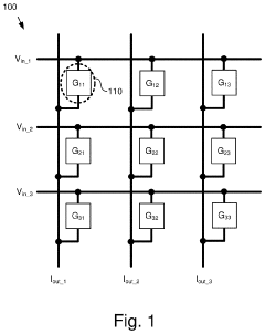
Neuromorphic chips are designed to mimic the structure and functionality of the human brain, utilizing neural networks and synaptic connections, whereas conventional semiconductors follow traditional von Neumann architecture with separate processing and memory units. This fundamental architectural difference allows neuromorphic chips to process information in a parallel, event-driven manner, making them more efficient for certain AI applications compared to the sequential processing of conventional semiconductors.- Neuromorphic architecture design and implementation: Neuromorphic chips are designed to mimic the structure and functionality of the human brain, using specialized architectures that differ significantly from conventional semiconductors. These designs incorporate neural networks, synaptic connections, and brain-inspired processing elements to enable efficient pattern recognition and learning capabilities. The architecture typically includes arrays of artificial neurons and synapses implemented in hardware, allowing for parallel processing and reduced power consumption compared to traditional computing approaches.
- Integration of neuromorphic elements with conventional semiconductor technology: Hybrid systems that combine neuromorphic computing elements with conventional semiconductor technology offer advantages of both paradigms. These integrated solutions incorporate brain-inspired neural circuits alongside traditional CMOS technology, enabling more efficient processing for specific applications while maintaining compatibility with existing computing infrastructure. The integration approaches include embedding neuromorphic cores within conventional chip designs, creating specialized co-processors, or developing interface layers that allow neuromorphic and conventional components to work together seamlessly.
- Materials and fabrication techniques for neuromorphic devices: Advanced materials and novel fabrication techniques are essential for creating efficient neuromorphic chips. These include memristive materials, phase-change materials, and specialized semiconductor compounds that can mimic synaptic behavior. The manufacturing processes often differ from conventional semiconductor fabrication, requiring precise control of material properties to achieve the desired neuromorphic functionality. These specialized materials enable features like non-volatile memory, analog computation, and spike-based signal processing that are fundamental to brain-inspired computing.
- Power efficiency and performance comparison: Neuromorphic chips offer significant advantages in power efficiency compared to conventional semiconductors for certain workloads, particularly those involving pattern recognition, sensory processing, and machine learning. These brain-inspired architectures can process information with much lower energy consumption by utilizing event-driven computation, local memory processing, and parallel architecture. Performance metrics and benchmarking methods have been developed to compare neuromorphic solutions against traditional computing approaches, highlighting the specific applications where each technology excels.
- Applications and use cases for neuromorphic computing: Neuromorphic chips are particularly well-suited for specific applications including edge computing, autonomous systems, real-time sensor processing, and artificial intelligence tasks. These applications leverage the inherent advantages of brain-inspired computing such as low power consumption, parallel processing, and efficient pattern recognition. Implementations range from smart sensors and IoT devices to advanced robotics systems and AI accelerators, where the unique capabilities of neuromorphic technology provide advantages over conventional semiconductor solutions.
02 Integration of memory and processing in neuromorphic designs
Neuromorphic chips integrate memory and processing elements in close proximity or within the same structure, similar to how neurons and synapses function in the brain. This integration helps overcome the von Neumann bottleneck present in conventional semiconductors where data transfer between separate memory and processing units creates performance limitations. By collocating memory and computation, neuromorphic designs achieve higher energy efficiency and reduced latency for neural network operations.Expand Specific Solutions03 Energy efficiency advantages of neuromorphic computing
Neuromorphic chips offer significant energy efficiency advantages over conventional semiconductors, particularly for AI workloads. These chips typically operate with event-driven or spike-based processing that activates circuits only when necessary, rather than the continuous clock-driven operation of traditional semiconductors. This approach, combined with analog or mixed-signal computing elements that perform calculations with lower precision but higher efficiency, enables neuromorphic systems to achieve orders of magnitude improvement in energy consumption for certain neural network applications.Expand Specific Solutions04 Materials and fabrication technologies for neuromorphic devices
Advanced materials and novel fabrication technologies are being developed specifically for neuromorphic computing devices. These include memristive materials, phase-change materials, and spintronic devices that can mimic synaptic behavior more efficiently than traditional CMOS technology. While conventional semiconductors primarily rely on established silicon-based fabrication processes, neuromorphic chips often incorporate these emerging materials alongside or instead of traditional semiconductors to achieve brain-like computing capabilities with improved density and efficiency.Expand Specific Solutions05 Hybrid systems combining neuromorphic and conventional semiconductor technologies
Hybrid computing systems that integrate both neuromorphic chips and conventional semiconductors are being developed to leverage the strengths of each technology. These systems typically use conventional processors for precise, general-purpose computing tasks while employing neuromorphic components for pattern recognition, sensory processing, and other brain-like functions. This complementary approach allows for efficient handling of diverse workloads, with the conventional components managing control flow and exact calculations while neuromorphic elements handle parallel, approximate computing tasks with high energy efficiency.Expand Specific Solutions
Leading Companies in Neuromorphic and Conventional Chip Industries
Neuromorphic computing is emerging as a disruptive technology in the semiconductor industry, currently in its early growth phase with an estimated market size of $69 million in 2023, projected to reach $8.4 billion by 2030. The competitive landscape features established players like IBM, Samsung, and HP developing advanced neuromorphic architectures, alongside specialized startups such as Syntiant and Polyn Technology focusing on edge AI applications. Academic-industry collaborations are accelerating, with research institutions like Tsinghua University and Fraunhofer-Gesellschaft partnering with corporations to bridge the gap between theoretical advances and commercial implementation. While conventional semiconductors still dominate computing, neuromorphic chips offer significant advantages in power efficiency and real-time processing for AI applications, though technical challenges in manufacturing scalability and programming paradigms remain barriers to widespread adoption.
SYNTIANT CORP
Technical Solution: Syntiant has developed the Neural Decision Processor (NDP), a specialized neuromorphic chip designed specifically for edge AI applications with extreme power efficiency. Unlike conventional semiconductors that separate memory and processing, Syntiant's architecture implements a neural network directly in silicon, with memory and computation integrated in a way that mimics brain function[7]. Their NDP100 and NDP200 series chips can perform deep learning inference while consuming less than 1mW of power, enabling always-on AI capabilities in battery-powered devices. Syntiant's technology uses a dataflow architecture where computations are triggered by incoming data rather than clock cycles, dramatically reducing power consumption compared to conventional processors. The company has demonstrated their chips performing complex audio recognition tasks while consuming 100-200 times less power than conventional microcontroller implementations[8]. Their latest generation chips can process multiple concurrent AI models for audio, vision, and sensor fusion applications.
Strengths: Ultra-low power consumption (sub-milliwatt) enabling always-on AI in battery-powered devices; purpose-built for edge deployment with minimal footprint; excellent performance for specific AI workloads like keyword spotting and sensor processing. Weaknesses: Limited to specific application domains rather than general-purpose computing; lower computational flexibility compared to programmable processors; requires specialized development tools and expertise.
International Business Machines Corp.
Technical Solution: IBM's TrueNorth neuromorphic chip represents one of the most significant advancements in the field, featuring a million programmable neurons and 256 million synapses organized into 4,096 neurosynaptic cores. The architecture implements an event-driven, parallel, and scalable design that mimics the brain's structure and function. TrueNorth operates at extremely low power consumption (70mW) while delivering the equivalent of 46 billion synaptic operations per second per watt, which is orders of magnitude more efficient than conventional von Neumann architectures[1]. IBM has further developed SyNAPSE (Systems of Neuromorphic Adaptive Plastic Scalable Electronics) technology that combines digital computation with analog memory to create a brain-inspired chip that can learn through experience rather than traditional programming[2]. This approach fundamentally differs from conventional semiconductors by processing information in a distributed, parallel manner rather than sequentially.
Strengths: Extremely low power consumption (15-300mW) compared to GPUs (250W+); highly parallel architecture enabling real-time sensory processing; scalable design allowing multiple chips to be tiled together. Weaknesses: Programming complexity requiring specialized knowledge; limited compatibility with existing software ecosystems; currently lower computational precision than conventional processors for certain numerical tasks.
Key Patents and Research in Brain-Inspired Computing
Hardware Accelerated Discretized Neural Network
PatentActiveUS20210334338A1
Innovation
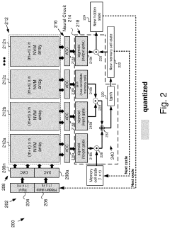
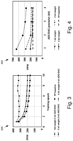
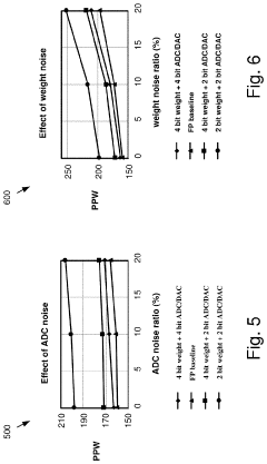
- A quantized neural network architecture that converts digital input and hidden state signals into analog form, processes them using non-volatile memory weight arrays for vector matrix multiplication, and then converts back to digital, with bit-widths reduced to 4 bits or less, utilizing DACs and ADCs to maintain performance comparable to 32-bit implementations.
Neuromorphic computing in dynamic random access memory
PatentActiveUS20200285945A1
Innovation
- Represents neurons by memory rows in DRAM, where each bit represents a synapse, and uses inherent decay properties to emulate brain-like learning by reinforcing or degrading synaptic states, offloading neural processing from CPUs to DRAM.
Energy Efficiency and Performance Metrics Analysis
Neuromorphic chips demonstrate remarkable energy efficiency advantages over conventional semiconductors, particularly in processing neural network workloads. While traditional von Neumann architecture-based processors consume significant power due to the constant shuttling of data between memory and processing units, neuromorphic designs minimize this energy expenditure through co-located memory and computation. Quantitative assessments reveal that neuromorphic solutions like IBM's TrueNorth and Intel's Loihi can achieve energy efficiencies of 1-100 picojoules per synaptic operation, representing orders of magnitude improvement over GPU and CPU implementations for similar neural network tasks.
Performance metrics for these architectures must be evaluated through different lenses. Conventional semiconductors excel in terms of raw computational throughput for general-purpose computing, typically measured in FLOPS (Floating Point Operations Per Second) or IPS (Instructions Per Second). In contrast, neuromorphic chips are optimized for specific neural processing metrics such as synaptic operations per second (SOPS) and synaptic operations per watt, which better reflect their efficiency in brain-inspired computing tasks.
Latency characteristics also differ significantly between these architectures. Neuromorphic systems often demonstrate superior performance in real-time processing scenarios requiring rapid response to sensory inputs, with some implementations achieving sub-millisecond latencies for complex pattern recognition tasks. This contrasts with conventional systems that may require substantial pre-processing and batch operations to achieve comparable results.
Scalability presents another important dimension for comparison. Conventional semiconductor technologies benefit from decades of manufacturing optimization but face increasing challenges with power density and heat dissipation as transistor counts grow. Neuromorphic architectures offer potentially superior scaling properties through their distributed, parallel processing approach, though current manufacturing techniques still limit their absolute scale compared to mainstream semiconductor products.
Application-specific benchmarking reveals that neuromorphic chips demonstrate particular advantages in edge computing scenarios where power constraints are severe. For instance, in always-on sensor processing applications, neuromorphic solutions can operate continuously while consuming only milliwatts of power, whereas conventional processors might require orders of magnitude more energy for equivalent functionality.
The efficiency gap becomes most pronounced in sparse, event-driven processing tasks that mimic biological neural activity patterns. In these scenarios, neuromorphic chips can achieve 100-1000x energy efficiency improvements by processing information only when relevant changes occur, rather than performing continuous computation cycles regardless of input significance.
Application Ecosystem Development for Neuromorphic Computing
The development of a robust application ecosystem is critical for the widespread adoption of neuromorphic computing technologies. Unlike conventional semiconductors that benefit from decades of established software frameworks, development tools, and application libraries, neuromorphic chips face significant challenges in ecosystem development due to their fundamentally different computing paradigm.
Current neuromorphic computing platforms are supported by specialized programming frameworks such as IBM's TrueNorth Neurosynaptic System, Intel's Loihi SDK, and BrainChip's development environment. These frameworks provide the necessary tools for implementing spiking neural networks (SNNs) but lack the maturity and breadth of conventional computing ecosystems like CUDA or TensorFlow.
Application development for neuromorphic systems requires specialized knowledge of event-based processing and spike-based information encoding, creating a steep learning curve for developers accustomed to traditional computing paradigms. This knowledge gap represents a significant barrier to adoption that must be addressed through comprehensive educational resources and simplified development interfaces.
Several promising application domains are emerging as natural fits for neuromorphic computing. Edge AI applications benefit from the low power consumption and real-time processing capabilities of neuromorphic chips. Sensory processing applications, particularly computer vision and audio processing, leverage the event-driven nature of neuromorphic systems to achieve efficient pattern recognition with minimal power requirements.
Industry collaborations are accelerating ecosystem development, with partnerships forming between neuromorphic hardware providers and application developers. Academic institutions are also contributing significantly by developing open-source tools and algorithms specifically designed for neuromorphic architectures.
Standardization efforts are beginning to emerge, though they remain in early stages. The development of common benchmarks, programming interfaces, and model formats would significantly accelerate ecosystem growth by enabling interoperability between different neuromorphic platforms and facilitating the transfer of applications across hardware implementations.
Looking forward, the convergence of neuromorphic computing with other emerging technologies presents exciting opportunities. Integration with quantum computing for specific optimization problems, combination with traditional AI accelerators in heterogeneous computing environments, and incorporation into IoT networks could create powerful new application paradigms that leverage the unique strengths of each technology.
Unlock deeper insights with Patsnap Eureka Quick Research — get a full tech report to explore trends and direct your research. Try now!
Generate Your Research Report Instantly with AI Agent
Supercharge your innovation with Patsnap Eureka AI Agent Platform!