Neuromorphic Chips in Next-Gen Semiconductor Technologies
OCT 9, 20259 MIN READ
Generate Your Research Report Instantly with AI Agent
PatSnap Eureka helps you evaluate technical feasibility & market potential.
Neuromorphic Computing Evolution and Objectives
Neuromorphic computing represents a paradigm shift in semiconductor technology, drawing inspiration from the human brain's neural architecture to create more efficient and powerful computing systems. The evolution of this field began in the late 1980s with Carver Mead's pioneering work at Caltech, where he first proposed using analog VLSI systems to mimic neurobiological architectures. This marked the birth of neuromorphic engineering as a distinct discipline bridging neuroscience and semiconductor technology.
Throughout the 1990s and early 2000s, research remained largely academic, with limited practical applications due to manufacturing constraints and insufficient understanding of neural processes. The field gained significant momentum around 2010 with the emergence of deep learning and renewed interest in artificial intelligence, creating demand for specialized hardware that could efficiently process neural network computations.
The development trajectory has been characterized by progressive improvements in energy efficiency, processing speed, and integration density. Early neuromorphic chips featured simple spiking neural networks with limited neurons and synapses, while contemporary designs incorporate billions of synaptic connections with sophisticated learning capabilities and dramatically reduced power consumption.
Key technological milestones include IBM's TrueNorth chip (2014), Intel's Loihi (2017), and BrainChip's Akida (2019), each representing significant advances in neuromorphic architecture implementation. These developments have progressively addressed fundamental challenges in signal processing, memory-compute integration, and power efficiency.
The primary objective of neuromorphic computing research is to develop semiconductor technologies that can process information with the efficiency and adaptability of biological neural systems while overcoming the limitations of traditional von Neumann architectures. Specific goals include achieving ultra-low power consumption (targeting milliwatt or even microwatt operation), enabling on-chip learning capabilities, and supporting massively parallel processing of unstructured data.
Looking forward, neuromorphic computing aims to enable a new generation of edge computing devices capable of real-time sensory processing, adaptive learning, and autonomous decision-making without cloud connectivity. The technology seeks to address the growing computational demands of artificial intelligence applications while dramatically reducing energy requirements compared to conventional approaches.
The convergence of advances in materials science, neuroscience understanding, and semiconductor fabrication techniques is creating unprecedented opportunities to realize practical neuromorphic systems that can transform computing paradigms across multiple industries.
Market Demand Analysis for Brain-Inspired Computing
The global market for brain-inspired computing solutions is experiencing unprecedented growth, driven by the increasing demand for more efficient and intelligent computing systems. Neuromorphic chips, which mimic the structure and functionality of the human brain, are positioned at the forefront of this revolution. Current market analysis indicates that the neuromorphic computing market is projected to grow significantly over the next decade, with applications spanning across multiple industries including artificial intelligence, robotics, healthcare, and autonomous vehicles.
The primary market drivers for neuromorphic chips stem from the limitations of traditional von Neumann architecture in handling complex AI workloads. As organizations increasingly deploy sophisticated machine learning models and neural networks, the demand for hardware that can process these workloads efficiently has surged. Neuromorphic chips offer substantial advantages in terms of power efficiency, processing speed for certain tasks, and the ability to learn and adapt—qualities that are highly valued in today's data-intensive environment.
Healthcare represents a particularly promising market segment, with applications in medical imaging analysis, patient monitoring systems, and drug discovery processes. The ability of neuromorphic systems to process sensory data in real-time while consuming minimal power makes them ideal for portable medical devices and implantable technologies.
In the automotive sector, the push toward autonomous vehicles has created substantial demand for neuromorphic solutions. These chips excel at processing visual data and making rapid decisions based on environmental inputs—critical capabilities for self-driving systems. Market research suggests that automotive applications could become one of the largest segments for neuromorphic technology within the next five years.
The consumer electronics industry is also showing increasing interest in neuromorphic computing, particularly for edge devices where power efficiency is paramount. Smart home systems, wearable technology, and mobile devices could all benefit from the reduced power consumption and improved AI capabilities that neuromorphic chips offer.
From a geographical perspective, North America currently leads the market due to substantial investments in research and development, followed closely by Asia-Pacific, where countries like China, Japan, and South Korea are making significant strides in semiconductor technology. Europe is also emerging as a key player, with several research institutions and companies focusing on neuromorphic computing solutions.
Despite the promising outlook, market adoption faces challenges related to software ecosystem development, integration with existing systems, and the need for standardized benchmarking methodologies. These factors currently limit widespread commercial deployment but are expected to be addressed as the technology matures and industry collaboration increases.
Neuromorphic Chip Technology Landscape and Barriers
The neuromorphic chip landscape is currently dominated by several key players, each with distinct approaches to brain-inspired computing. IBM's TrueNorth represents one of the pioneering architectures with its million-neuron design, while Intel's Loihi has advanced the field with its self-learning capabilities and scalable architecture. Qualcomm's Zeroth NPU and BrainChip's Akida focus on edge computing applications, demonstrating the industry's shift toward energy-efficient, distributed intelligence solutions.
Academic institutions like Stanford, MIT, and the University of Manchester have established significant research programs, often collaborating with industry partners to bridge theoretical advances with practical implementations. These collaborations have accelerated development in areas such as spiking neural networks (SNNs) and memristive technologies.
Despite promising advances, neuromorphic computing faces substantial barriers to widespread adoption. The most significant technical challenge remains the development of reliable, scalable memory technologies that can effectively mimic synaptic plasticity. Current memristor implementations suffer from variability issues, limited endurance, and integration difficulties with CMOS processes. These challenges have constrained the scaling potential of neuromorphic systems.
Another critical barrier is the lack of standardized programming models and development tools. Unlike traditional computing paradigms with established languages and frameworks, neuromorphic computing requires fundamentally different approaches to algorithm design and implementation. This has created a significant knowledge gap and steep learning curve for developers interested in leveraging these technologies.
Power efficiency, while theoretically superior to conventional architectures, remains problematic in practice. Current neuromorphic implementations still consume more energy than theoretical models predict, particularly when scaling to complex applications. This efficiency gap must be addressed before neuromorphic chips can fulfill their promise for ultra-low-power computing.
Manufacturing complexity presents another substantial barrier. The integration of novel materials and device structures with traditional semiconductor fabrication processes introduces yield challenges and reliability concerns. Many promising neuromorphic technologies require specialized fabrication techniques that are difficult to scale to commercial production volumes.
The ecosystem surrounding neuromorphic computing remains underdeveloped compared to traditional computing platforms. Limited software support, few application-specific libraries, and minimal developer resources have slowed adoption outside specialized research environments. This ecosystem gap represents perhaps the most significant non-technical barrier to widespread implementation of neuromorphic technologies in next-generation semiconductor products.
Current Neuromorphic Chip Design Approaches
01 Neuromorphic architecture design
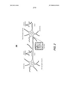
Neuromorphic chips are designed to mimic the structure and functionality of the human brain, using specialized architectures that integrate processing and memory. These designs typically feature networks of artificial neurons and synapses that enable parallel processing and event-driven computation. The architecture allows for efficient handling of neural network operations while significantly reducing power consumption compared to traditional computing approaches.- Neuromorphic architecture design: Neuromorphic chips are designed to mimic the structure and functionality of the human brain, incorporating neural networks and synaptic connections. These architectures enable parallel processing, energy efficiency, and adaptive learning capabilities. The designs typically include arrays of artificial neurons and synapses that can process information in ways similar to biological neural systems, allowing for more efficient handling of complex cognitive tasks and pattern recognition.
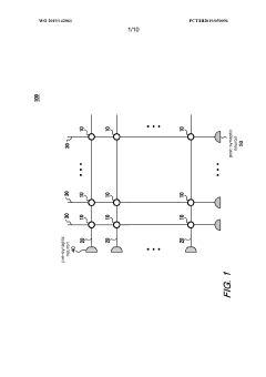
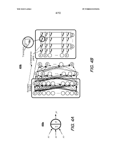
- Memristor-based neuromorphic computing: Memristors are used as key components in neuromorphic chips to simulate synaptic behavior. These devices can change their resistance based on the history of current flow, enabling them to store and process information simultaneously. Memristor-based neuromorphic systems offer advantages in power efficiency, density, and the ability to implement spike-timing-dependent plasticity (STDP) learning rules, making them suitable for edge computing applications and artificial intelligence tasks that require low power consumption.
- Spiking neural networks implementation: Spiking neural networks (SNNs) are implemented in neuromorphic chips to more accurately replicate the communication method of biological neurons. These networks use discrete spikes or pulses to transmit information, rather than continuous values, resulting in more energy-efficient computation. SNN implementations in hardware enable event-driven processing, where computation occurs only when needed, and can adapt to temporal patterns in data, making them particularly suitable for real-time sensory processing and dynamic environments.
- On-chip learning and adaptation mechanisms: Neuromorphic chips incorporate on-chip learning capabilities that allow them to adapt to new data without requiring external training. These mechanisms include hardware implementations of learning algorithms such as spike-timing-dependent plasticity (STDP), reinforcement learning, and unsupervised learning techniques. On-chip learning enables continuous adaptation to changing environments, reduces the need for cloud connectivity, and allows for personalization of AI systems while maintaining privacy by processing data locally.
- Integration with sensors and edge computing: Neuromorphic chips are designed to integrate directly with sensors for efficient processing of sensory data at the edge. This integration enables real-time processing of visual, auditory, and other sensory inputs with minimal power consumption. By processing data close to the source, these systems reduce latency and bandwidth requirements while enhancing privacy. Applications include smart cameras, autonomous vehicles, wearable devices, and IoT systems that require intelligent, low-power processing of sensory information in real-time environments.
02 Memristor-based implementations
Memristors are key components in many neuromorphic chip designs, serving as artificial synapses that can change their resistance based on the history of current flow. These devices enable efficient implementation of synaptic plasticity and learning mechanisms. Memristor-based neuromorphic systems offer advantages in terms of power efficiency, density, and the ability to perform in-memory computing, eliminating the bottleneck between memory and processing units.Expand Specific Solutions03 Spiking neural networks implementation
Neuromorphic chips often implement spiking neural networks (SNNs) that communicate through discrete events or spikes, similar to biological neurons. This approach enables energy-efficient computation as processing occurs only when necessary. SNN implementations on neuromorphic hardware can achieve significant power savings while maintaining computational capabilities for pattern recognition, classification, and other AI tasks.Expand Specific Solutions04 On-chip learning and adaptation
Advanced neuromorphic chips incorporate on-chip learning capabilities that allow the system to adapt and improve over time without external training. These chips implement various learning algorithms such as spike-timing-dependent plasticity (STDP) and other biologically-inspired mechanisms. On-chip learning enables edge computing applications where devices can learn from their environment and adapt to new conditions without requiring cloud connectivity.Expand Specific Solutions05 Application-specific neuromorphic systems
Neuromorphic chips are being developed for specific applications such as computer vision, speech recognition, autonomous vehicles, and IoT devices. These application-specific designs optimize the neuromorphic architecture for particular tasks, balancing performance, power consumption, and size constraints. Specialized neuromorphic systems can achieve orders of magnitude improvement in energy efficiency compared to conventional processors when performing AI tasks in their target domains.Expand Specific Solutions
Leading Companies and Research Institutions in Neuromorphic Computing
Neuromorphic chip technology is currently in the early growth phase of its industry lifecycle, characterized by rapid innovation and increasing commercial applications. The global market for neuromorphic computing is projected to reach $8-10 billion by 2028, growing at a CAGR of approximately 25%. From a technical maturity perspective, major players like IBM, Intel, and Samsung are leading with advanced research platforms, while specialized companies such as Syntiant, Polyn Technology, and Lingxi Technology are developing application-specific neuromorphic solutions. Academic institutions including Tsinghua University and KAIST are contributing fundamental research, creating a diverse ecosystem. The technology is transitioning from research laboratories to commercial applications, particularly in edge AI, autonomous systems, and energy-efficient computing, though widespread adoption remains several years away.
International Business Machines Corp.
Technical Solution: IBM's TrueNorth neuromorphic chip architecture represents one of the most advanced implementations in the field, featuring a million programmable neurons and 256 million synapses organized into 4,096 neurosynaptic cores[1]. The chip mimics the brain's structure with event-driven processing that activates only when needed, consuming just 70mW during real-time operation. IBM has further evolved this technology with their more recent NorthPole design, which improves energy efficiency to 4.5 trillion synaptic operations per second per watt (TOPS/W)[2]. IBM's neuromorphic approach implements spiking neural networks (SNNs) that process information through discrete spikes rather than continuous signals, enabling efficient pattern recognition and sensory processing applications. The architecture supports on-chip learning through spike-timing-dependent plasticity (STDP) mechanisms, allowing the system to adapt to new data without requiring complete retraining[3].
Strengths: Exceptional energy efficiency (orders of magnitude better than conventional architectures); scalable design allowing for multi-chip systems; mature development ecosystem with programming tools. Weaknesses: Limited compatibility with traditional deep learning frameworks; requires specialized programming approaches; higher implementation complexity compared to conventional digital designs.
SYNTIANT CORP
Technical Solution: Syntiant has developed the Neural Decision Processors (NDP) series, which represents a hybrid approach combining neuromorphic principles with traditional digital design. Their NDP200 chip can process multiple concurrent audio streams while consuming less than 1mW of power[1]. Unlike pure neuromorphic designs, Syntiant's architecture focuses on optimizing specific neural network operations for always-on applications, particularly in speech recognition and sensor fusion. The company's technology implements a memory-centric computing approach where computation happens within memory arrays, dramatically reducing the energy costs associated with data movement between separate processing and memory units[2]. Syntiant's chips feature a programmable tensor accelerator optimized for deep learning models, with particular emphasis on convolutional neural networks and recurrent neural networks commonly used in audio processing. Their architecture supports quantized neural networks with 1-8 bit precision, allowing for efficient implementation of complex models in resource-constrained environments[3].
Strengths: Ultra-low power consumption ideal for battery-powered devices; optimized for specific high-value applications like voice activation; production-ready technology already deployed in commercial products. Weaknesses: Less flexible than general-purpose neuromorphic designs; primarily focused on audio applications rather than broader neuromorphic computing; limited support for unsupervised learning paradigms.
Key Patents and Breakthroughs in Neuromorphic Engineering
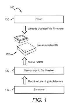
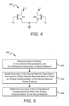
Systems And Methods For Determining Circuit-Level Effects On Classifier Accuracy
PatentActiveUS20190065962A1
Innovation
- The development of neuromorphic chips that simulate 'silicon' neurons, processing information in parallel with bursts of electric current at non-uniform intervals, and the use of systems and methods to model the effects of circuit-level characteristics on neural networks, such as thermal noise and weight inaccuracies, to optimize their performance.
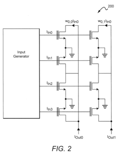
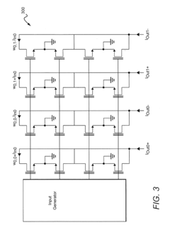
Neuromorphic chip for updating precise synaptic weight values
PatentWO2019142061A1
Innovation
- A neuromorphic chip with a crossbar array configuration that uses resistive devices and switches to express synaptic weights with a variable number of resistive elements, allowing for precise synaptic weight updates by dynamically connecting axon lines and assigning weights to synaptic cells, thereby mitigating device variability and maintaining training power and speed.
Energy Efficiency Benchmarks and Optimization Strategies
Energy efficiency has emerged as a critical benchmark for evaluating neuromorphic chips within next-generation semiconductor technologies. Current neuromorphic architectures demonstrate significant advantages over traditional von Neumann computing systems, with leading designs achieving power efficiency improvements of 100-1000x for specific neural network workloads. The SpiNNaker2 neuromorphic system, for instance, delivers approximately 10 TOPS/W (Tera Operations Per Second per Watt), while IBM's TrueNorth architecture achieves around 46 GOPS/W (Giga Operations Per Second per Watt) for sparse neural network computations.
Benchmark methodologies for neuromorphic chips require specialized approaches that differ from conventional semiconductor testing. Standard metrics include energy per synaptic operation (measured in picojoules), static power consumption, and computational efficiency for specific neural network tasks. Recent industry testing frameworks have begun incorporating neuromorphic-specific workloads that emphasize temporal information processing and event-driven computation to provide more accurate efficiency comparisons.
Several optimization strategies have demonstrated promising results for enhancing energy efficiency in neuromorphic designs. At the architectural level, implementing fine-grained power gating techniques allows for selective activation of neural circuits only when processing is required. This approach has yielded up to 40% power reduction in recent experimental designs. Sparse computing techniques that activate components only when necessary have further reduced power consumption by 30-60% in benchmark tests.
Material innovations represent another frontier for efficiency improvements. The integration of novel materials such as hafnium oxide for memristive devices has demonstrated potential for reducing the energy required for synaptic operations to femtojoule levels. Additionally, three-dimensional integration techniques that stack memory elements directly above processing units minimize data movement energy costs, which typically account for 60-80% of total system energy in conventional architectures.
Dynamic voltage and frequency scaling (DVFS) techniques adapted specifically for neuromorphic workloads have shown particular promise. These approaches dynamically adjust operating parameters based on computational demands, with recent implementations demonstrating additional 25-35% energy savings without significant performance degradation. Emerging research in approximate computing techniques tailored to neuromorphic architectures suggests potential for further efficiency gains by exploiting the inherent error tolerance of many neural algorithms.
Integration Challenges with Conventional Computing Systems
The integration of neuromorphic chips with conventional computing systems presents significant technical challenges that must be addressed for successful deployment in next-generation semiconductor technologies. Traditional von Neumann architectures operate on fundamentally different principles than neuromorphic systems, creating compatibility issues at multiple levels of the computing stack.
At the hardware level, neuromorphic chips typically utilize specialized memory structures and unique signaling mechanisms that mimic biological neural networks. These components often operate with different voltage levels, timing protocols, and data formats compared to conventional CMOS-based systems. The physical interface between these disparate technologies requires sophisticated bridge circuits and signal conversion mechanisms that can introduce latency and power overhead.
Data representation poses another critical challenge. Conventional computing systems process information using binary logic and fixed-point or floating-point number formats, while neuromorphic systems often employ spike-based encoding or other bio-inspired representations. This fundamental difference necessitates complex translation layers that can preserve information fidelity while enabling efficient communication between the two paradigms.
Programming models and software frameworks for neuromorphic systems remain in early developmental stages compared to the mature ecosystem supporting conventional computing. Developers face significant barriers when attempting to partition applications across neuromorphic and conventional components, as existing tools provide limited support for heterogeneous execution environments. The lack of standardized APIs and middleware solutions further complicates integration efforts.
System-level resource management presents additional complications. Neuromorphic chips typically exhibit different power profiles, thermal characteristics, and performance scaling properties compared to conventional processors. Existing operating systems and resource schedulers are not designed to optimize workloads across such heterogeneous computing elements, potentially leading to inefficient resource utilization and suboptimal performance.
Verification and testing methodologies must also evolve to accommodate neuromorphic components. Traditional digital testing approaches may be insufficient for validating the analog behaviors and probabilistic computing elements often found in neuromorphic designs. This gap necessitates new testing paradigms and quality assurance frameworks to ensure reliable operation in integrated systems.
Despite these challenges, promising research directions are emerging. Hardware abstraction layers specifically designed for neuromorphic-conventional interfaces, unified programming frameworks that support both computing paradigms, and adaptive runtime systems capable of intelligently managing heterogeneous resources represent potential solutions to these integration challenges.
Unlock deeper insights with PatSnap Eureka Quick Research — get a full tech report to explore trends and direct your research. Try now!
Generate Your Research Report Instantly with AI Agent
Supercharge your innovation with PatSnap Eureka AI Agent Platform!