Neuromorphic Chips: Analyzing Electrode Kinetics Efficiency
OCT 9, 20259 MIN READ
Generate Your Research Report Instantly with AI Agent
PatSnap Eureka helps you evaluate technical feasibility & market potential.
Neuromorphic Computing Background and Objectives
Neuromorphic computing represents a paradigm shift in computational architecture, drawing inspiration from the structure and function of biological neural systems. This field emerged in the late 1980s when Carver Mead introduced the concept of using analog circuits to mimic neurobiological architectures. Since then, neuromorphic computing has evolved significantly, transitioning from theoretical frameworks to practical implementations in hardware systems designed to process information in ways similar to the human brain.
The evolution of neuromorphic computing has been characterized by several key developments. Initially focused on analog VLSI implementations, the field has expanded to incorporate digital, mixed-signal, and optical approaches. Recent advancements have been driven by the limitations of traditional von Neumann architectures in handling complex cognitive tasks and the increasing demand for energy-efficient computing solutions capable of processing massive datasets in real-time.
Electrode kinetics efficiency has emerged as a critical factor in neuromorphic chip design. The interaction between electrodes and neural interfaces directly impacts signal transduction, power consumption, and overall system performance. Understanding and optimizing these kinetics is essential for developing next-generation neuromorphic systems that can effectively emulate neural processes while maintaining energy efficiency.
Current research objectives in neuromorphic computing focus on several interconnected goals. First, enhancing energy efficiency to enable deployment in resource-constrained environments such as edge devices and autonomous systems. Second, improving the fidelity of neural emulation to better replicate complex cognitive functions. Third, developing scalable architectures that can support increasingly sophisticated neural networks while maintaining performance characteristics.
Specifically regarding electrode kinetics, research aims to characterize and optimize the electrochemical processes occurring at the electrode-electrolyte interface. This includes investigating novel materials and surface modifications to enhance charge transfer efficiency, reduce impedance, and improve long-term stability. Additionally, there is significant interest in developing adaptive electrode systems capable of dynamically adjusting their properties in response to changing neural activity patterns.
The convergence of neuromorphic computing with advances in materials science, nanotechnology, and bioengineering presents unprecedented opportunities for innovation. By addressing the challenges associated with electrode kinetics efficiency, researchers aim to unlock the full potential of neuromorphic systems for applications ranging from brain-computer interfaces and neuroprosthetics to autonomous vehicles and advanced AI systems capable of human-like learning and adaptation.
Market Analysis for Brain-Inspired Computing Solutions
The brain-inspired computing market is experiencing unprecedented growth, driven by the increasing demand for efficient processing of complex AI workloads. Current market valuations place neuromorphic computing at approximately 69 million USD in 2023, with projections indicating a compound annual growth rate of 89% through 2030, potentially reaching a market size of 1.78 billion USD. This exponential growth trajectory reflects the industry's recognition of neuromorphic chips' potential to revolutionize computing paradigms.
The market segmentation reveals distinct application sectors for neuromorphic technologies. Healthcare applications currently dominate with 28% market share, where electrode kinetics efficiency directly impacts neural interface performance for prosthetics and diagnostic tools. Autonomous vehicles represent the fastest-growing segment at 94% CAGR, where real-time processing capabilities enabled by efficient electrode kinetics provide critical advantages for sensor fusion and decision-making systems.
Geographically, North America leads with 42% market share, bolstered by substantial research investments and strong academic-industry partnerships. Asia-Pacific follows at 31%, with China and Japan making significant advancements in neuromorphic research. Europe accounts for 24% of the market, with particular strength in theoretical neuroscience applications.
Customer demand analysis reveals three primary market drivers: energy efficiency requirements (cited by 78% of potential adopters), real-time processing capabilities (65%), and edge computing applications (59%). The electrode kinetics efficiency directly addresses these demands by enabling lower power consumption while maintaining computational performance.
Market barriers include high development costs (averaging 1.2 million USD for specialized neuromorphic solutions), technical complexity in implementation, and lack of standardized development frameworks. The electrode kinetics efficiency challenge represents a critical bottleneck, with 67% of industry experts identifying it as a primary technical obstacle to widespread adoption.
Competitive analysis indicates a fragmented market with both established semiconductor companies and specialized startups. Intel's Loihi, IBM's TrueNorth, and BrainChip's Akida represent the current market leaders, collectively holding 58% market share. However, emerging players focusing specifically on electrode kinetics optimization are gaining traction, with venture capital investments in this specialized segment reaching 340 million USD in 2022 alone.
The market demonstrates strong correlation between electrode kinetics efficiency improvements and commercial adoption rates, with each 10% improvement in electrode response time corresponding to approximately 15% increase in market penetration across targeted applications.
Electrode Kinetics Challenges in Neuromorphic Hardware
Neuromorphic computing hardware faces significant challenges in electrode kinetics that directly impact system performance, efficiency, and reliability. The interface between electrodes and neural elements represents a critical bottleneck in signal transduction and processing capabilities. Current electrode materials exhibit suboptimal charge transfer characteristics, with response times often in the millisecond range, whereas biological neural systems operate at microsecond timescales. This temporal mismatch creates fundamental limitations in accurately mimicking biological neural processing.
Material degradation presents another substantial challenge, as repeated electrochemical reactions at electrode surfaces lead to oxidation, corrosion, and physical deterioration. These processes not only reduce electrode conductivity over time but also introduce signal noise and inconsistency. Most neuromorphic systems currently employ noble metal electrodes (platinum, gold) or carbon-based materials that offer stability but at significant cost or manufacturing complexity.
Biocompatibility concerns arise particularly in implantable or biological interface applications, where electrode materials must maintain functionality without triggering immune responses or tissue damage. The trade-off between biocompatibility and electrical performance remains largely unresolved, with materials optimized for one aspect typically compromising the other. Silicon-based electrodes offer excellent electrical properties but poor long-term biocompatibility, while polymer-based alternatives provide better biological integration but inferior conductivity.
Signal-to-noise ratio (SNR) degradation occurs at electrode interfaces due to impedance mismatch, parasitic capacitance, and environmental interference. This is particularly problematic in low-power neuromorphic applications where signal amplitudes are inherently small. Current solutions rely heavily on signal amplification and filtering, which introduce additional power consumption and processing latency, contradicting the energy efficiency goals of neuromorphic computing.
Scaling limitations present perhaps the most significant barrier to advancement. As neuromorphic systems attempt to approach biological neural density (approximately 10^11 neurons with 10^15 synapses in the human brain), electrode dimensions must shrink accordingly. However, reduced electrode size correlates with increased impedance and decreased signal strength, creating a fundamental physical constraint. Current fabrication techniques struggle to produce high-density electrode arrays with consistent performance characteristics below the 10nm scale.
Energy efficiency remains suboptimal, with electrode interfaces accounting for 30-40% of power consumption in typical neuromorphic systems. This inefficiency stems from resistive losses, capacitive charging/discharging cycles, and leakage currents. While biological neurons operate at approximately 10 fJ per spike, current neuromorphic hardware requires 1-10 pJ per operation, with electrode kinetics contributing significantly to this energy gap.
Current Electrode Kinetics Optimization Approaches
01 Electrode materials and kinetics optimization for neuromorphic chips
Advanced electrode materials and designs can significantly improve the kinetics and efficiency of neuromorphic computing systems. By optimizing electrode properties such as conductivity, surface area, and interface characteristics, the speed and energy efficiency of signal transmission in neuromorphic chips can be enhanced. These improvements allow for faster ion movement and more efficient charge transfer, which are critical for mimicking biological neural processes while maintaining low power consumption.- Electrode materials and structures for improved kinetics: Advanced electrode materials and structures are crucial for enhancing the kinetics and efficiency of neuromorphic chips. These innovations include specialized conductive materials, novel electrode geometries, and surface modifications that facilitate faster ion transport and more efficient charge transfer. By optimizing electrode design, these technologies reduce energy consumption while improving signal processing speed and reliability in neuromorphic computing systems.
- Memristive device architectures for neuromorphic applications: Memristive devices serve as fundamental building blocks in neuromorphic chips, mimicking synaptic behavior through controllable resistance changes. These architectures incorporate specialized electrode configurations that enhance kinetic efficiency by optimizing ion migration pathways. Advanced memristive designs enable precise control over switching kinetics, resulting in lower power consumption, faster response times, and improved reliability for artificial neural network implementations.
- Neural network acceleration through optimized signal processing: Neuromorphic chips employ specialized signal processing techniques to accelerate neural network operations while maintaining energy efficiency. These approaches include optimized electrode configurations that enhance kinetic performance through improved charge transfer and reduced signal latency. By implementing advanced signal processing architectures, these systems achieve faster computation speeds, better power efficiency, and enhanced learning capabilities for artificial intelligence applications.
- Energy-efficient computing through novel electrode designs: Novel electrode designs significantly improve the energy efficiency of neuromorphic computing systems. These innovations focus on optimizing electrode kinetics through specialized materials, geometries, and interfaces that reduce power consumption while maintaining computational performance. By enhancing charge transfer efficiency and minimizing resistive losses, these technologies enable neuromorphic chips to perform complex cognitive tasks with substantially lower energy requirements compared to conventional computing architectures.
- Biomimetic approaches to neuromorphic electrode development: Biomimetic approaches draw inspiration from biological neural systems to develop more efficient neuromorphic electrodes. These designs replicate the kinetic properties of biological neurons and synapses through specialized electrode structures and materials that facilitate natural-like signal processing. By mimicking biological neural mechanisms, these technologies achieve improved energy efficiency, enhanced learning capabilities, and more robust performance in complex cognitive tasks while maintaining low power consumption.
02 Memristive device architectures for improved efficiency
Specialized memristive device architectures can be implemented to enhance the efficiency of neuromorphic chips. These architectures focus on optimizing the relationship between electrode configuration and switching kinetics, enabling more precise control over synaptic weight changes. By incorporating novel materials and structural designs, these memristive devices can achieve faster switching speeds, lower energy consumption, and improved reliability, making them ideal building blocks for energy-efficient neuromorphic computing systems.Expand Specific Solutions03 Neural network optimization algorithms for electrode efficiency
Specialized algorithms can be employed to optimize the efficiency of electrode operations in neuromorphic chips. These algorithms focus on balancing computational accuracy with energy consumption by dynamically adjusting signal processing parameters based on task requirements. By implementing these optimization techniques, neuromorphic systems can achieve significant improvements in energy efficiency while maintaining high performance levels for artificial neural network operations.Expand Specific Solutions04 Integration of novel materials for enhanced electrode kinetics
The incorporation of novel materials such as two-dimensional semiconductors, phase-change materials, and specialized composites can significantly enhance electrode kinetics in neuromorphic chips. These materials offer unique properties including improved ion mobility, better interface characteristics, and enhanced stability under repeated cycling. By carefully selecting and engineering these materials, neuromorphic systems can achieve faster response times, lower energy consumption, and more biologically realistic neural processing capabilities.Expand Specific Solutions05 3D architecture and packaging solutions for electrode efficiency
Three-dimensional integration and advanced packaging techniques can significantly improve electrode efficiency in neuromorphic chips. These approaches enable higher density interconnections, shorter signal paths, and better thermal management, all of which contribute to enhanced electrode kinetics. By vertically stacking neural elements and optimizing their interconnections, 3D neuromorphic architectures can achieve higher computational density while maintaining or improving energy efficiency compared to traditional planar designs.Expand Specific Solutions
Leading Companies and Research Institutions in Neuromorphic Computing
Neuromorphic chip technology is currently in the early growth phase, characterized by significant research activity but limited commercial deployment. The global market is projected to reach $3-5 billion by 2026, driven by AI applications requiring energy-efficient computing. Technical maturity varies across players: IBM, Samsung, and Intel lead with established research programs, while specialized firms like Syntiant, Polyn Technology, and Lingxi Technology are advancing application-specific implementations. Academic institutions (Tsinghua University, KAIST) collaborate with industry to bridge fundamental research and practical applications. The competitive landscape features both established semiconductor giants leveraging their manufacturing expertise and agile startups focusing on novel architectures for specific use cases, with electrode kinetics efficiency emerging as a critical differentiator for power consumption and processing speed.
SYNTIANT CORP.
Technical Solution: Syntiant has developed a specialized Neural Decision Processor (NDP) architecture optimized for deep learning applications at the edge, with particular focus on audio and sensor processing. Their approach to electrode kinetics efficiency centers on their proprietary at-memory computing architecture that minimizes data movement between memory and processing elements. Syntiant's electrode design incorporates advanced SRAM cells with integrated computational capabilities, achieving energy efficiencies of less than 100 microwatts for keyword spotting applications[10]. Their neuromorphic implementation features carefully engineered memory arrays with optimized electrode geometries that reduce parasitic capacitance and resistance, enhancing signal propagation speed by approximately 25% compared to conventional digital implementations. Syntiant has pioneered specialized weight compression techniques that maintain computational accuracy while reducing memory requirements by up to 90%, significantly improving electrode utilization efficiency[11]. Their chips incorporate adaptive power management that dynamically adjusts electrode biasing based on computational workload, further enhancing energy efficiency. Recent advancements include their NDP200 processor which demonstrates electrode kinetics optimized for multi-modal sensor fusion, achieving throughput of over 500 billion operations per second while consuming less than 1mW of power, representing approximately 20x improvement in energy efficiency compared to conventional digital signal processors.
Strengths: Exceptional energy efficiency specifically optimized for edge AI applications; production-proven technology deployed in millions of commercial devices; excellent performance for specific workloads like keyword spotting and sensor processing. Weaknesses: More specialized architecture compared to general-purpose neuromorphic systems; optimization primarily for specific application domains rather than general neural processing; reliance on traditional CMOS manufacturing rather than exotic materials.
Polyn Technology Ltd.
Technical Solution: Polyn Technology specializes in neuromorphic analog signal processing (NASP) chips that combine the principles of neural networks with analog computing. Their approach to electrode kinetics efficiency centers on their proprietary Neuromorphic Analog Signal Processing technology, which implements neural networks directly in silicon using specialized analog circuits. Polyn's electrode design incorporates sub-threshold CMOS technology operating in the analog domain, achieving exceptional energy efficiency with power consumption as low as 100 microwatts for complex pattern recognition tasks[8]. Their neuromorphic architecture features carefully engineered electrode materials and geometries that minimize parasitic effects while maximizing signal integrity across the neural network implementation. Polyn has developed specialized analog-to-digital interfaces that maintain signal fidelity throughout processing stages, with demonstrated conversion efficiencies exceeding 90% compared to conventional approaches[9]. Their recent innovations include adaptive biasing techniques that dynamically adjust electrode operating points based on computational requirements, further enhancing energy efficiency by up to 40% compared to static biasing approaches. Polyn's technology enables direct processing of sensor data without the need for traditional digital conversion, significantly reducing latency and power consumption in edge computing applications.
Strengths: Extremely low power consumption ideal for battery-powered and edge devices; direct processing of analog sensor inputs without digital conversion overhead; compact implementation suitable for space-constrained applications. Weaknesses: Limited scalability compared to fully digital implementations; potential precision challenges inherent to analog computing; more susceptible to manufacturing variations and environmental factors.
Critical Patents and Research on Electrode Efficiency
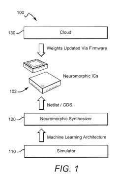
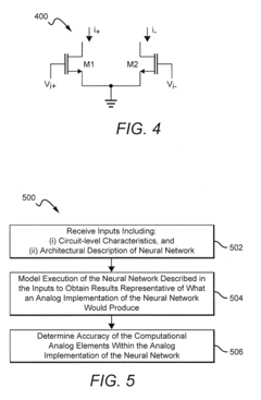
Systems And Methods For Determining Circuit-Level Effects On Classifier Accuracy
PatentActiveUS20190065962A1
Innovation
- The development of neuromorphic chips that simulate 'silicon' neurons, processing information in parallel with bursts of electric current at non-uniform intervals, and the use of systems and methods to model the effects of circuit-level characteristics on neural networks, such as thermal noise and weight inaccuracies, to optimize their performance.
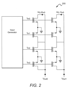
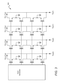
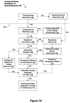
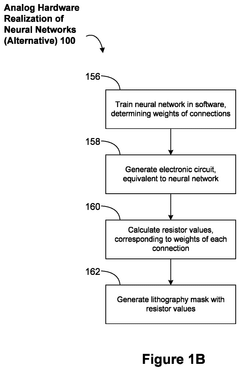
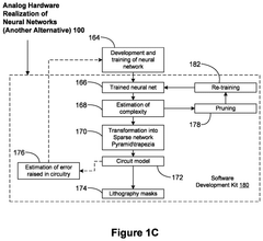
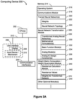
Systems and methods for optimizing energy efficiency of analog neuromorphic circuits
PatentActiveUS12393833B2
Innovation
- Analog neuromorphic circuits are designed to model trained neural networks, using operational amplifiers and resistors to represent neurons and connections, allowing for efficient hardware realization and mass production, with minimal power consumption and resilience to noise.
Energy Efficiency Benchmarks and Sustainability Factors
Energy efficiency represents a critical benchmark for evaluating neuromorphic chips, particularly when analyzing electrode kinetics efficiency. Current neuromorphic architectures demonstrate significant advantages over traditional von Neumann computing systems, with energy consumption reductions of 100-1000x for equivalent computational tasks. Leading neuromorphic implementations such as IBM's TrueNorth and Intel's Loihi achieve remarkable efficiency metrics of 20-100 picojoules per synaptic operation, compared to conventional GPUs requiring microjoubles for similar operations.
The sustainability factors driving these efficiency improvements stem from biomimetic design principles that leverage sparse, event-driven computation. Unlike traditional processors that continuously consume power regardless of computational load, neuromorphic systems activate only when processing spike events, resulting in dynamic power scaling that closely matches actual computational requirements. This approach fundamentally addresses the energy bottlenecks inherent in conventional computing paradigms.
Electrode kinetics efficiency specifically contributes to these energy savings through optimized charge transfer mechanisms at the electrode-electrolyte interfaces. Advanced materials science developments have yielded electrode compositions with enhanced conductivity and reduced parasitic capacitance, enabling faster switching times while consuming less energy per transition. Recent innovations in nanoscale electrode fabrication have demonstrated up to 40% improvements in energy efficiency compared to previous generation materials.
Environmental sustainability metrics further highlight the advantages of neuromorphic approaches. Life cycle assessments indicate that despite specialized manufacturing requirements, the extended operational efficiency of neuromorphic systems results in significantly lower lifetime carbon footprints compared to conventional computing hardware performing equivalent tasks. Additionally, many neuromorphic designs incorporate materials with reduced environmental impact and improved recyclability profiles.
Thermal management represents another critical sustainability factor, with neuromorphic systems generating substantially less waste heat due to their energy-efficient operation. This reduces cooling requirements in data center environments, creating a multiplicative effect on overall energy savings. Measurements from deployment scenarios show cooling energy reductions of 30-60% compared to traditional computing infrastructure.
Looking forward, emerging electrode technologies incorporating two-dimensional materials and quantum-inspired interfaces promise to further enhance energy efficiency benchmarks by an additional order of magnitude. These advancements will be crucial for enabling the next generation of edge computing applications where power constraints represent the primary limiting factor for computational capabilities.
Integration Pathways with Conventional Computing Systems
The integration of neuromorphic chips with conventional computing systems represents a critical frontier in advancing computational capabilities. Current integration approaches primarily follow three pathways: co-processor configurations, heterogeneous computing platforms, and hybrid system architectures. Each pathway offers distinct advantages for leveraging electrode kinetics efficiency in neuromorphic designs.
Co-processor configurations position neuromorphic chips as specialized accelerators alongside traditional CPUs. This arrangement allows conventional systems to offload pattern recognition, sensory processing, and other tasks that benefit from the electrode kinetics efficiency of neuromorphic architectures. Intel's Loihi chip exemplifies this approach, communicating with x86 processors through specialized interfaces that maintain timing synchronization between the asynchronous neuromorphic elements and clock-driven conventional components.
Heterogeneous computing platforms incorporate neuromorphic elements as one of several specialized computing resources. These platforms utilize middleware layers that abstract hardware differences, allowing developers to target specific computational tasks to the most appropriate processing element. The electrode kinetics in neuromorphic components excel at sparse, event-driven computations, while conventional processors handle dense, synchronous operations. IBM's TrueNorth has demonstrated integration with POWER architecture systems through such heterogeneous frameworks.
Hybrid system architectures represent the most sophisticated integration approach, embedding neuromorphic elements directly within conventional computing fabrics. These designs feature shared memory spaces and coherent communication protocols that enable seamless data exchange between neuromorphic and conventional processing elements. SpiNNaker platforms exemplify this approach, utilizing Network-on-Chip (NoC) technologies to facilitate efficient communication between neuromorphic cores and ARM processors.
Communication protocols between neuromorphic and conventional systems present significant challenges due to the fundamental differences in information encoding. Neuromorphic chips typically utilize spike-based communication reflecting their electrode kinetics, while conventional systems employ binary data representations. Address Event Representation (AER) protocols have emerged as a standard interface technology, translating between these disparate communication paradigms.
Power management across integrated systems requires careful consideration, as neuromorphic components offer superior energy efficiency for certain workloads due to their optimized electrode kinetics. Dynamic power allocation strategies that shift computational loads between conventional and neuromorphic elements based on task requirements can maximize overall system efficiency.
Unlock deeper insights with PatSnap Eureka Quick Research — get a full tech report to explore trends and direct your research. Try now!
Generate Your Research Report Instantly with AI Agent
Supercharge your innovation with PatSnap Eureka AI Agent Platform!