

Compare Flowless Lithography Vs Computational Lithography: Benefits
APR 24, 20268 MIN READ
Generate Your Research Report Instantly with AI Agent
Patsnap Eureka helps you evaluate technical feasibility & market potential.
Flowless vs Computational Lithography Background and Objectives
Lithography technology has undergone significant evolution since its inception in the semiconductor industry, serving as the cornerstone for manufacturing integrated circuits with ever-decreasing feature sizes. Traditional lithography processes have relied on photoresist materials and complex chemical processing steps to pattern semiconductor wafers. However, as the industry approaches physical limits imposed by wavelength constraints and material properties, innovative approaches have emerged to address these fundamental challenges.
Flowless lithography represents a paradigm shift from conventional photoresist-based patterning methods. This technology eliminates the need for liquid photoresist application, development, and removal processes that have been standard in semiconductor manufacturing for decades. Instead, flowless lithography employs direct material modification techniques, utilizing focused energy beams to selectively alter substrate properties without requiring chemical processing steps. This approach fundamentally reimagines the patterning process by removing the intermediate photoresist layer entirely.
Computational lithography, conversely, enhances traditional lithography through advanced mathematical modeling and algorithmic optimization. This technology leverages sophisticated software algorithms to predict and compensate for optical proximity effects, mask errors, and process variations. By incorporating machine learning techniques and complex mathematical models, computational lithography optimizes mask designs, exposure conditions, and process parameters to achieve superior pattern fidelity and yield enhancement.
The primary objective of comparing these technologies centers on evaluating their respective capabilities in addressing current semiconductor manufacturing challenges. Key performance metrics include resolution enhancement, process complexity reduction, manufacturing cost optimization, and scalability for future technology nodes. Both approaches aim to extend lithography capabilities beyond traditional limits while maintaining manufacturing feasibility.
The comparative analysis seeks to determine optimal application scenarios for each technology, considering factors such as pattern complexity, throughput requirements, and integration challenges with existing manufacturing infrastructure. Understanding the fundamental differences between direct material modification and computational enhancement approaches provides crucial insights for strategic technology adoption decisions in advanced semiconductor manufacturing environments.
Market Demand for Advanced Lithography Solutions
The semiconductor industry faces unprecedented demand for advanced lithography solutions driven by the relentless pursuit of smaller node geometries and higher device densities. As traditional photolithography approaches physical limitations at sub-7nm processes, manufacturers are actively seeking innovative alternatives that can deliver superior resolution, reduced defect rates, and enhanced manufacturing efficiency. This technological inflection point has created substantial market opportunities for both flowless lithography and computational lithography approaches.
Market dynamics reveal strong adoption momentum for computational lithography solutions across leading foundries and memory manufacturers. Major semiconductor companies are investing heavily in computational correction techniques, including optical proximity correction, source mask optimization, and inverse lithography technology. These solutions address critical manufacturing challenges such as pattern fidelity, edge placement accuracy, and yield optimization that become increasingly severe at advanced nodes.
The flowless lithography segment demonstrates emerging market traction, particularly among companies developing next-generation manufacturing processes. Early adopters are drawn to its potential for eliminating traditional photoresist-related defects and enabling direct pattern transfer capabilities. This approach appeals to manufacturers seeking to reduce process complexity while maintaining high-resolution patterning performance.
Regional market distribution shows concentrated demand in Asia-Pacific, particularly Taiwan, South Korea, and China, where major foundries and memory manufacturers operate advanced fabrication facilities. North American and European markets contribute significantly through equipment suppliers and research institutions developing cutting-edge lithography technologies.
Application-specific demand varies considerably across market segments. Logic device manufacturers prioritize computational lithography for its proven ability to enhance existing infrastructure investments and improve yield rates. Memory manufacturers show balanced interest in both approaches, evaluating flowless lithography for its potential cost advantages in high-volume production scenarios.
The total addressable market continues expanding as semiconductor content increases across automotive, artificial intelligence, and Internet of Things applications. This growth trajectory sustains robust demand for advanced lithography solutions capable of enabling next-generation device architectures and performance requirements.
Current State and Challenges in Lithography Technologies
The lithography industry currently stands at a critical juncture where traditional photolithography approaches are reaching fundamental physical limitations. As semiconductor manufacturing pushes toward sub-3nm nodes, conventional optical lithography faces unprecedented challenges in achieving the required resolution, pattern fidelity, and manufacturing throughput. The industry has increasingly relied on complex multi-patterning techniques, extreme ultraviolet (EUV) lithography, and sophisticated computational corrections to maintain Moore's Law progression.
Current lithography systems predominantly utilize immersion ArF lithography at 193nm wavelength, supplemented by EUV lithography at 13.5nm for the most advanced nodes. These systems require extensive computational lithography techniques including optical proximity correction (OPC), source mask optimization (SMO), and inverse lithography technology (ILT) to compensate for optical diffraction effects and process variations. The computational overhead has grown exponentially, with mask data preparation times extending to weeks for complex designs.
Manufacturing costs have escalated dramatically, with EUV systems costing over $200 million per unit and requiring substantial infrastructure investments. Mask costs for advanced nodes now exceed $5 million per layer, creating significant barriers for smaller volume productions. The industry faces a productivity crisis where the time and cost required for mask generation and process optimization increasingly limit design flexibility and time-to-market.
Process variability remains a persistent challenge, with line edge roughness, critical dimension uniformity, and overlay accuracy becoming increasingly difficult to control at atomic scales. Current lithography systems struggle with stochastic effects that become more pronounced as feature sizes approach molecular dimensions. These variations directly impact device performance and yield, requiring extensive process monitoring and correction mechanisms.
Emerging applications in advanced packaging, MEMS, and photonics demand greater flexibility in pattern generation and reduced setup times. Traditional mask-based approaches lack the agility required for rapid prototyping and customized manufacturing. The semiconductor industry increasingly requires lithography solutions that can adapt quickly to design changes while maintaining high resolution and throughput capabilities for next-generation device architectures.
Existing Flowless and Computational Lithography Solutions
01 Computational lithography for optical proximity correction and resolution enhancement
Computational lithography techniques are employed to perform optical proximity correction (OPC) and resolution enhancement to improve pattern fidelity and critical dimension control. These methods use mathematical models and algorithms to predict and compensate for optical effects during the lithography process, enabling more accurate pattern transfer at advanced technology nodes. The computational approaches optimize mask designs and exposure parameters to achieve better imaging results without requiring changes to the physical lithography hardware.- Computational lithography for optical proximity correction and resolution enhancement: Computational lithography techniques are employed to perform optical proximity correction (OPC) and resolution enhancement to improve pattern fidelity and critical dimension control. These methods use advanced algorithms to predict and compensate for optical effects during the lithography process, enabling more accurate pattern transfer at smaller feature sizes. The computational approach allows for optimization of mask designs and exposure parameters to achieve better imaging results.
- Flowless lithography systems with improved throughput and uniformity: Flowless lithography systems eliminate the need for traditional flow-based processes, resulting in improved throughput and better uniformity across the substrate. These systems utilize advanced exposure techniques and optimized stage movements to achieve consistent patterning without requiring continuous flow of materials. The approach reduces process complexity and enhances manufacturing efficiency while maintaining high pattern quality.
- Machine learning and artificial intelligence in computational lithography optimization: Machine learning and artificial intelligence algorithms are integrated into computational lithography workflows to optimize various aspects of the lithography process. These techniques enable rapid prediction of lithography outcomes, automated optimization of process parameters, and intelligent correction of pattern distortions. The use of advanced computational methods significantly reduces the time required for mask optimization and process development.
- Multi-patterning and source-mask optimization techniques: Advanced computational lithography incorporates multi-patterning strategies and source-mask optimization to extend the capabilities of existing lithography equipment. These techniques involve decomposing complex patterns into multiple simpler exposures and co-optimizing the illumination source and mask patterns simultaneously. The combined approach enables the printing of features beyond the conventional resolution limits of the lithography system.
- Defect detection and process control in computational lithography: Computational lithography methods incorporate advanced defect detection and process control mechanisms to ensure manufacturing quality. These systems use simulation and modeling to predict potential defects before actual production and implement real-time monitoring and feedback control during the lithography process. The integration of computational analysis with process control enables early detection of issues and rapid correction, improving yield and reducing manufacturing costs.
02 Flowless lithography systems with reduced fluid management complexity
Flowless lithography approaches eliminate or minimize the need for continuous fluid flow during immersion lithography processes. These systems reduce the complexity associated with fluid supply, circulation, and removal mechanisms, thereby simplifying equipment design and maintenance. By managing fluid presence more efficiently or using alternative exposure methods, flowless systems can reduce defects related to fluid dynamics and improve throughput while maintaining high resolution capabilities.Expand Specific Solutions03 Machine learning and artificial intelligence in computational lithography optimization
Advanced computational lithography leverages machine learning and artificial intelligence algorithms to optimize lithography processes and mask synthesis. These intelligent systems can learn from historical process data to predict optimal correction strategies, accelerate computation times, and improve pattern accuracy. The integration of neural networks and deep learning models enables more sophisticated analysis of complex lithographic phenomena and automated optimization of multiple process parameters simultaneously.Expand Specific Solutions04 Source-mask optimization for enhanced lithographic performance
Source-mask optimization (SMO) is a computational lithography technique that simultaneously optimizes both the illumination source and mask patterns to maximize imaging performance. This co-optimization approach considers the interaction between source characteristics and mask features to achieve better process windows, improved depth of focus, and enhanced pattern fidelity. The method enables extension of existing lithography equipment capabilities to smaller feature sizes without requiring new hardware investments.Expand Specific Solutions05 Defect reduction and yield improvement through computational methods
Computational lithography techniques contribute to defect reduction and yield improvement by predicting and preventing potential printing errors before actual wafer exposure. These methods analyze mask designs for hotspots, systematic defects, and process margin issues, enabling early correction in the design phase. By simulating various process conditions and identifying weak points in patterns, computational approaches help optimize manufacturability and reduce costly rework cycles in semiconductor fabrication.Expand Specific Solutions
Key Players in Lithography Equipment and Software Industry
The lithography landscape represents a mature industry undergoing significant technological transition, with the market experiencing robust growth driven by advanced semiconductor manufacturing demands. The industry has reached a critical inflection point where traditional flowless lithography approaches are being enhanced and, in some cases, replaced by sophisticated computational lithography solutions. Technology maturity varies significantly across market players, with ASML Netherlands BV leading in advanced EUV systems, while companies like Synopsys and NVIDIA drive computational innovation through AI-enhanced modeling and simulation platforms. Chinese manufacturers including SMIC, Shanghai Microelectronics Equipment, and Hua Hong Semiconductor are rapidly advancing their capabilities, though primarily focused on mature node technologies. Research institutions like Imec, Cornell University, and ETH Zurich continue pushing technological boundaries, while established players such as FUJIFILM and Kodak leverage decades of optical expertise. The competitive dynamics reflect a bifurcated market where computational approaches are becoming essential for sub-7nm processes, creating opportunities for software-centric solutions alongside traditional hardware-intensive manufacturing.
ASML Netherlands BV
Technical Solution: ASML leads in computational lithography through advanced optical proximity correction (OPC) and source mask optimization (SMO) technologies. Their computational approach enables sub-7nm node manufacturing by using sophisticated algorithms to predict and correct pattern distortions before exposure. The company's Brion division specializes in computational lithography software that optimizes mask designs and illumination conditions to achieve precise pattern transfer. ASML's EUV lithography systems integrate computational methods to handle complex curvilinear mask shapes and advanced resolution enhancement techniques, enabling high-volume manufacturing of leading-edge semiconductors with improved yield and reduced defect rates.
Strengths: Market leadership in EUV technology, comprehensive computational lithography software suite, proven high-volume manufacturing capability. Weaknesses: High system costs, complex computational requirements demanding significant processing power and time.
Synopsys, Inc.
Technical Solution: Synopsys provides comprehensive computational lithography solutions through their Sentaurus Lithography and Proteus platforms, offering advanced OPC, inverse lithography technology (ILT), and machine learning-enhanced process optimization. Their computational approach enables mask synthesis optimization, hotspot detection, and process window enhancement for advanced nodes. The company's solutions integrate with design-for-manufacturing flows, providing early-stage lithography-aware design optimization. Synopsys leverages AI and machine learning algorithms to accelerate computational lithography tasks while maintaining accuracy, supporting both traditional immersion and EUV lithography processes with advanced curvilinear mask optimization capabilities.
Strengths: Comprehensive EDA ecosystem integration, advanced AI-driven optimization algorithms, strong design-manufacturing co-optimization capabilities. Weaknesses: Software-focused approach requires partnership with equipment vendors, high computational resource requirements for complex optimizations.
Core Innovations in Flowless Lithography Technologies
Large scale computational lithography using machine learning models
PatentActiveUS12249115B2
Innovation
- The use of machine learning models to infer aerial images and resist profiles, replacing the need for computationally expensive physical models, thereby speeding up the simulation process while maintaining accuracy.


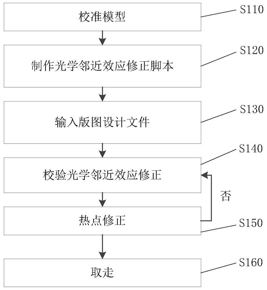
Computational lithography method and system for optical proximity correction
PatentActiveCN109932864B
Innovation
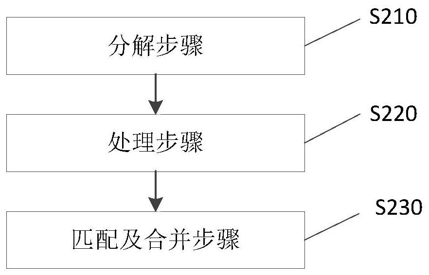
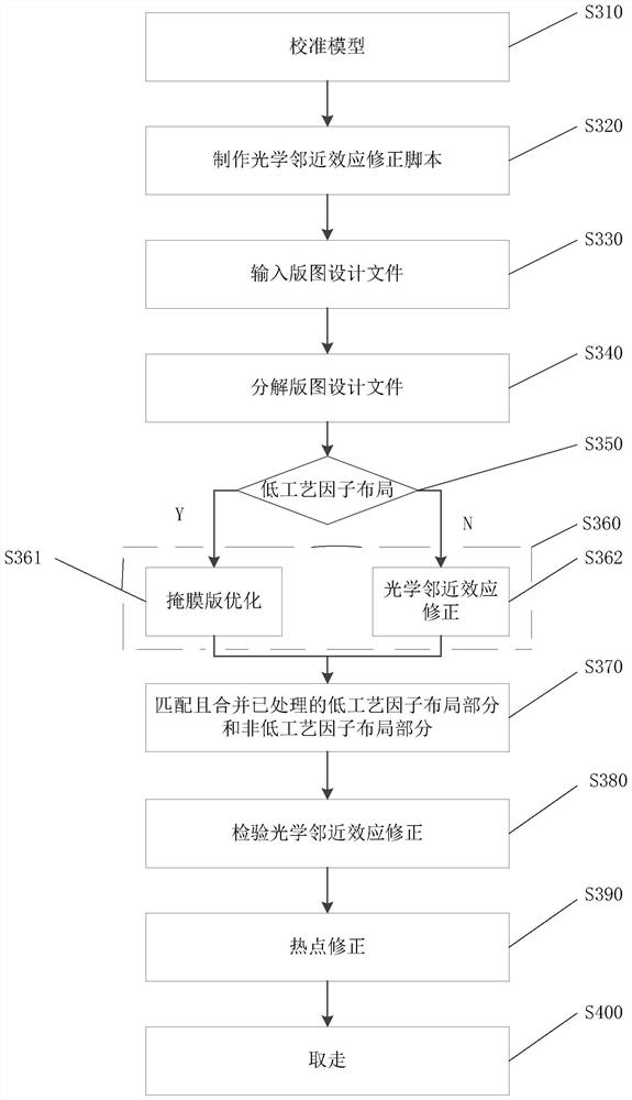
- By decomposing the layout design file into a first layout part with a process factor lower than the preset threshold and a second layout part with a process factor higher than the preset threshold, and processing and merging the two parts respectively, iteration steps are reduced and processing efficiency is improved.

Cost-Benefit Analysis of Lithography Approaches
The economic evaluation of flowless lithography versus computational lithography reveals distinct cost structures and return profiles that significantly impact manufacturing decisions. Flowless lithography systems require substantial upfront capital investment, with advanced EUV systems costing between $150-200 million per unit. However, these systems demonstrate superior throughput capabilities, processing 140-170 wafers per hour, which translates to lower per-wafer processing costs in high-volume production scenarios.
Computational lithography approaches present a fundamentally different cost paradigm. While the initial hardware investment is considerably lower, ranging from $50-80 million for advanced immersion systems, the operational expenses are dominated by computational infrastructure and software licensing costs. The computational overhead requires dedicated high-performance computing clusters, with annual operating costs reaching $10-15 million for state-of-the-art facilities processing advanced node geometries.
The total cost of ownership analysis demonstrates that flowless lithography achieves cost parity at production volumes exceeding 50,000 wafers per month. Below this threshold, computational lithography maintains economic advantages due to its lower fixed costs and greater process flexibility. The break-even point shifts favorably toward flowless systems when considering multi-year depreciation cycles and the reduced need for complex optical proximity correction algorithms.
Yield considerations significantly influence the economic equation. Flowless lithography typically achieves 2-3% higher yield rates due to reduced process variability, translating to substantial cost savings in advanced semiconductor manufacturing where individual wafers can represent thousands of dollars in material costs. Conversely, computational lithography offers superior design rule flexibility, enabling manufacturers to optimize layouts for specific applications without hardware modifications.
The scalability factor presents another critical economic dimension. Flowless systems demonstrate linear cost scaling with capacity expansion, while computational approaches face exponential increases in processing time and computational requirements as feature sizes decrease. This relationship becomes particularly pronounced at sub-5nm nodes, where computational lithography processing times can exceed 24 hours per mask layer compared to 2-3 hours for equivalent flowless approaches.
Performance Metrics and Quality Assessment Framework
Establishing a comprehensive performance metrics and quality assessment framework for comparing flowless lithography and computational lithography requires standardized evaluation criteria that capture both technical capabilities and practical implementation outcomes. The framework must encompass resolution accuracy, throughput efficiency, defect density measurements, and process stability indicators to provide objective comparative analysis between these two advanced lithography approaches.
Resolution performance serves as the primary metric, measured through critical dimension uniformity (CDU), line edge roughness (LER), and pattern fidelity across various feature sizes. Flowless lithography demonstrates superior performance in maintaining consistent feature dimensions without flow-induced distortions, while computational lithography excels in complex pattern correction through algorithmic optimization. Both technologies require evaluation using standardized test patterns including dense lines, isolated features, and two-dimensional structures.
Throughput assessment involves measuring wafer processing rates, computational overhead, and total cycle time from design to final pattern transfer. Flowless lithography typically exhibits faster physical processing due to reduced material handling steps, whereas computational lithography introduces variable processing times depending on pattern complexity and correction algorithm sophistication. The framework must account for these temporal variations when establishing fair comparison baselines.
Defect characterization encompasses systematic detection and classification of pattern defects, including missing features, bridging, and dimensional variations. Quality metrics should incorporate defect density per unit area, defect size distribution, and critical defect identification rates. Flowless systems generally produce fewer material-related defects, while computational approaches may introduce algorithm-induced artifacts requiring specialized detection methodologies.
Process window analysis evaluates robustness across varying operational conditions, including dose latitude, focus tolerance, and environmental stability. The assessment framework should incorporate statistical process control methods, measuring process capability indices and yield correlation factors. Long-term stability monitoring through repeated measurements ensures consistent performance evaluation and identifies potential degradation patterns specific to each lithography approach.
Unlock deeper insights with Patsnap Eureka Quick Research — get a full tech report to explore trends and direct your research. Try now!
Generate Your Research Report Instantly with AI Agent
Supercharge your innovation with Patsnap Eureka AI Agent Platform!