

How to Optimize Computational Lithography for Yield
APR 24, 20269 MIN READ
Generate Your Research Report Instantly with AI Agent
Patsnap Eureka helps you evaluate technical feasibility & market potential.
Computational Lithography Background and Yield Optimization Goals
Computational lithography has emerged as a critical technology in semiconductor manufacturing, representing the convergence of advanced optical physics, mathematical modeling, and computational algorithms to enable precise pattern transfer onto silicon wafers. This field encompasses sophisticated techniques including optical proximity correction (OPC), inverse lithography technology (ILT), source mask optimization (SMO), and resolution enhancement technologies (RET) that collectively address the fundamental challenges of printing increasingly complex patterns at dimensions approaching the physical limits of light wavelengths.
The evolution of computational lithography stems from the industry's relentless pursuit of Moore's Law scaling, where traditional optical lithography approaches became insufficient to maintain pattern fidelity and manufacturing yield at advanced technology nodes. As feature sizes shrunk below the wavelength of exposure light, proximity effects, optical diffraction, and process variations began significantly impacting the ability to reproduce intended circuit patterns accurately on wafers.
Modern computational lithography systems integrate multiple optimization algorithms that work synergistically to predict and compensate for various manufacturing effects. These systems must account for complex interactions between mask patterns, illumination conditions, lens aberrations, resist chemistry, and substrate topography. The computational models have evolved from simple geometric corrections to sophisticated physical simulations that incorporate electromagnetic field calculations, photoresist kinetics, and etch process modeling.
The primary goal of yield optimization in computational lithography centers on maximizing the percentage of functional chips produced per wafer while maintaining acceptable performance characteristics. This objective requires balancing multiple competing factors including pattern fidelity, critical dimension uniformity, overlay accuracy, and defect density across the entire wafer surface and throughout the manufacturing process window.
Yield optimization strategies focus on enhancing process robustness through improved pattern predictability and reduced sensitivity to manufacturing variations. Key targets include minimizing edge placement errors, controlling line width roughness, reducing hotspot formation, and ensuring adequate process margins for focus and exposure dose variations. Advanced optimization frameworks now incorporate machine learning algorithms and statistical methods to predict yield-limiting patterns and automatically generate correction strategies.
The ultimate technical objectives encompass achieving sub-nanometer edge placement accuracy, maintaining critical dimension uniformity within tight specifications across diverse pattern densities, and ensuring robust printability under realistic manufacturing conditions. These goals require continuous advancement in computational algorithms, model accuracy, and optimization methodologies to support next-generation semiconductor device manufacturing requirements.
Market Demand for Advanced Lithography Yield Enhancement
The semiconductor industry faces unprecedented pressure to enhance lithography yield as device geometries continue shrinking toward sub-3nm nodes. Advanced computational lithography has emerged as a critical enabler for maintaining manufacturing viability at these extreme dimensions, where traditional optical proximity correction approaches reach fundamental limitations.
Market demand for computational lithography yield enhancement solutions is primarily driven by the economic imperative of foundries and integrated device manufacturers. As wafer processing costs escalate exponentially with each technology node, even marginal yield improvements translate to substantial financial benefits. Leading foundries report that single-digit percentage improvements in yield can generate hundreds of millions in additional revenue annually.
The proliferation of artificial intelligence, high-performance computing, and mobile applications creates sustained demand for advanced semiconductors manufactured at cutting-edge nodes. This market pressure intensifies the need for sophisticated computational lithography techniques that can predict and compensate for manufacturing variations before they impact production yield.
Memory manufacturers represent another significant demand driver, particularly as 3D NAND and advanced DRAM architectures require increasingly precise pattern fidelity. The transition to extreme ultraviolet lithography has created new challenges in computational modeling, as traditional resist models prove inadequate for EUV photochemistry and stochastic effects.
Automotive and industrial sectors are increasingly adopting advanced semiconductor technologies for autonomous driving and Industry 4.0 applications. These markets demand exceptional reliability and yield consistency, creating opportunities for computational lithography solutions that can ensure robust manufacturing across process variations.
The geographic distribution of demand reflects the concentration of advanced semiconductor manufacturing. Asia-Pacific regions, particularly Taiwan, South Korea, and China, represent the largest market segments due to their dominant foundry and memory manufacturing presence. North American and European markets focus primarily on specialized applications and research-driven implementations.
Emerging applications in quantum computing, photonics integration, and advanced packaging technologies are creating new market segments for computational lithography yield enhancement. These applications often require novel patterning approaches that challenge conventional lithography paradigms, driving demand for innovative computational solutions.
The market exhibits strong growth momentum as manufacturers recognize that computational lithography optimization is no longer optional but essential for economic viability at advanced nodes. This recognition has transformed computational lithography from a research curiosity into a mission-critical manufacturing capability.
Current State and Challenges in Computational Lithography Yield
Computational lithography has emerged as a critical enabler for advanced semiconductor manufacturing, particularly as feature sizes continue to shrink below the wavelength of exposure light. The current state of computational lithography encompasses several mature technologies including Optical Proximity Correction (OPC), Source Mask Optimization (SMO), and Resolution Enhancement Techniques (RET). These technologies have successfully enabled the production of nodes down to 5nm and below, demonstrating remarkable progress in overcoming fundamental physical limitations.
However, the industry faces unprecedented challenges in maintaining and improving yield as geometries approach atomic scales. Process variations have become increasingly problematic, with even minor fluctuations in temperature, pressure, or chemical concentrations causing significant yield degradation. The stochastic effects of photon shot noise and molecular-level resist behavior introduce random variations that are difficult to predict and control through traditional computational methods.
Edge placement error (EPE) has emerged as one of the most critical yield-limiting factors in advanced nodes. Current computational lithography tools struggle to accurately predict and compensate for the complex interactions between mask patterns, optical systems, and resist chemistry that contribute to EPE. The computational burden of full-chip simulation with sufficient accuracy to capture these effects often exceeds practical time and resource constraints for high-volume manufacturing.
Mask complexity represents another significant challenge, with modern photomasks containing billions of features requiring sophisticated correction algorithms. The computational intensity of optimizing these complex patterns while maintaining manufacturability constraints has pushed existing algorithms to their limits. Traditional rule-based approaches are increasingly inadequate for handling the non-linear interactions present in extreme ultraviolet (EUV) lithography systems.
The integration of multiple patterning techniques, such as self-aligned double patterning (SADP) and self-aligned quadruple patterning (SAQP), has introduced additional layers of complexity. Each patterning step introduces its own sources of variation, and the cumulative effect of these variations across multiple exposures creates yield challenges that current computational models struggle to accurately predict and optimize.
Furthermore, the transition to EUV lithography has introduced new physical phenomena including mask 3D effects, flare, and stochastic defects that require fundamentally different computational approaches. Existing computational lithography frameworks, originally developed for deep ultraviolet systems, require substantial modifications to address these EUV-specific challenges while maintaining the speed and accuracy required for production environments.
Existing Solutions for Lithography Yield Optimization
01 Optical proximity correction (OPC) techniques for yield improvement
Computational lithography methods employ optical proximity correction algorithms to compensate for diffraction effects and process variations in photolithography. These techniques modify mask patterns to ensure that the printed features on wafers match the intended design more accurately. By optimizing the mask layout through iterative simulations and corrections, manufacturing yield can be significantly improved as critical dimensions are better controlled across the wafer.- Optical proximity correction (OPC) techniques for yield improvement: Computational lithography methods employ optical proximity correction algorithms to compensate for diffraction effects and process variations in photolithography. These techniques modify mask patterns to ensure that the printed features on wafers match the intended design more accurately. By optimizing the mask layout through iterative simulations and corrections, manufacturing yield can be significantly improved as critical dimensions are better controlled across the wafer.
- Source-mask optimization (SMO) for lithography enhancement: Advanced computational methods simultaneously optimize both the illumination source and mask patterns to maximize lithography performance. This co-optimization approach considers the interaction between source characteristics and mask features to achieve better pattern fidelity and process windows. The technique enables higher yield by expanding the manufacturing tolerance and reducing sensitivity to process variations.
- Machine learning and AI-based lithography optimization: Artificial intelligence and machine learning algorithms are applied to predict and optimize lithography outcomes. These methods can learn from historical manufacturing data to identify patterns and correlations that affect yield. By training models on large datasets, the systems can predict hotspots, recommend corrections, and optimize process parameters more efficiently than traditional rule-based approaches.
- Process window analysis and hotspot detection: Computational tools analyze the lithography process window to identify regions where patterns are susceptible to manufacturing defects. These methods simulate various process conditions to detect potential failure points before actual fabrication. Early identification of problematic areas allows designers to make corrections that prevent yield loss, ensuring robust manufacturing across process variations.
- Inverse lithography technology (ILT) for mask synthesis: Inverse lithography approaches work backward from the desired wafer pattern to determine optimal mask shapes. Unlike conventional correction methods, these techniques treat mask synthesis as an inverse problem, using computational algorithms to generate mask patterns that produce the best possible wafer results. This methodology can achieve superior pattern fidelity and larger process margins, directly contributing to higher manufacturing yield.
02 Source-mask optimization (SMO) for lithography enhancement
Advanced computational methods simultaneously optimize both the illumination source and mask patterns to maximize lithography performance. This co-optimization approach considers the interaction between source characteristics and mask features to achieve better pattern fidelity and process windows. The technique enables higher resolution patterning and improved yield by finding optimal combinations that traditional sequential optimization cannot achieve.Expand Specific Solutions03 Machine learning and AI-based lithography optimization
Artificial intelligence and machine learning algorithms are applied to predict lithography outcomes and optimize process parameters. These methods can learn from historical manufacturing data to identify patterns and correlations that affect yield. By training models on large datasets, the systems can predict hotspots, recommend corrections, and accelerate the optimization process compared to traditional physics-based simulations.Expand Specific Solutions04 Process window analysis and hotspot detection
Computational tools analyze the robustness of lithography processes across various manufacturing conditions to identify potential failure points. These methods simulate how pattern features respond to variations in focus, exposure dose, and other process parameters. Early detection of problematic layout patterns allows designers to make corrections before manufacturing, thereby preventing yield loss from systematic defects.Expand Specific Solutions05 Inverse lithography technology (ILT) for mask synthesis
Inverse lithography approaches work backward from the desired wafer pattern to determine optimal mask shapes using computational algorithms. Unlike rule-based correction methods, these techniques treat mask optimization as an inverse problem, allowing for more complex and freeform mask patterns. This methodology can achieve superior pattern fidelity and larger process margins, leading to improved manufacturing yield for advanced technology nodes.Expand Specific Solutions
Key Players in Computational Lithography and EDA Industry
The computational lithography optimization market is experiencing rapid growth driven by increasing demand for advanced semiconductor nodes and yield enhancement requirements. The industry has reached a mature development stage with established market leaders including ASML Netherlands BV dominating EUV lithography systems, while foundries like Taiwan Semiconductor Manufacturing Co. and GlobalFoundries drive implementation demands. Technology maturity varies significantly across segments, with companies like Synopsys, Cadence Design Systems, and Siemens Industry Software leading in EDA solutions for computational lithography, while Applied Materials and Toshiba provide critical manufacturing equipment. Asian players including Semiconductor Manufacturing International (Shanghai) Corp. and ChangXin Memory Technologies represent emerging competitive forces, particularly in cost-effective solutions. Research institutions like Beijing Institute of Technology and Institute of Microelectronics of Chinese Academy of Sciences contribute to algorithm development, while specialized firms like Dongfang Jingyuan Electron and Takumi Technology focus on yield management and design-for-manufacturing solutions, indicating a highly segmented but technologically mature competitive landscape.
ASML Netherlands BV
Technical Solution: ASML develops advanced computational lithography solutions integrated with their EUV and DUV lithography systems. Their approach combines sophisticated optical proximity correction (OPC) algorithms with machine learning-based process optimization to enhance yield performance. The company's computational lithography platform utilizes advanced source mask optimization (SMO) techniques and incorporates real-time process control feedback loops. Their solutions feature predictive modeling capabilities that account for lens aberrations, mask effects, and resist behavior to minimize critical dimension variations and improve pattern fidelity across the wafer.
Strengths: Market-leading lithography equipment with integrated computational solutions, extensive process knowledge, strong R&D capabilities. Weaknesses: High cost of ownership, complex system integration requirements, dependency on advanced node processes.
Applied Materials, Inc.
Technical Solution: Applied Materials develops computational lithography optimization solutions integrated with their process equipment and metrology systems. Their approach combines advanced process modeling with real-time feedback control to optimize lithographic yield. The company's solutions feature predictive analytics that utilize machine learning algorithms to analyze process variations and automatically adjust parameters for optimal yield outcomes. Their computational lithography platform integrates with inspection and metrology tools to provide closed-loop process control, enabling continuous optimization of critical dimensions, overlay accuracy, and defect reduction across high-volume manufacturing environments.
Strengths: Integrated equipment and software solutions, strong process control expertise, comprehensive metrology capabilities. Weaknesses: Equipment-centric approach may limit flexibility, high capital investment requirements, complex system integration across different lithography platforms.
Core Innovations in Computational Lithography Algorithms
A computational photolithography method
PatentActiveCN112083631B
Innovation
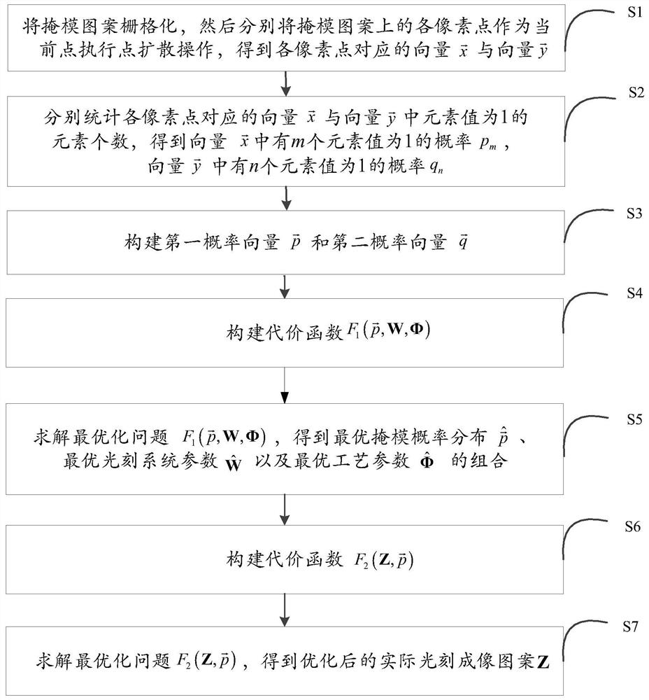
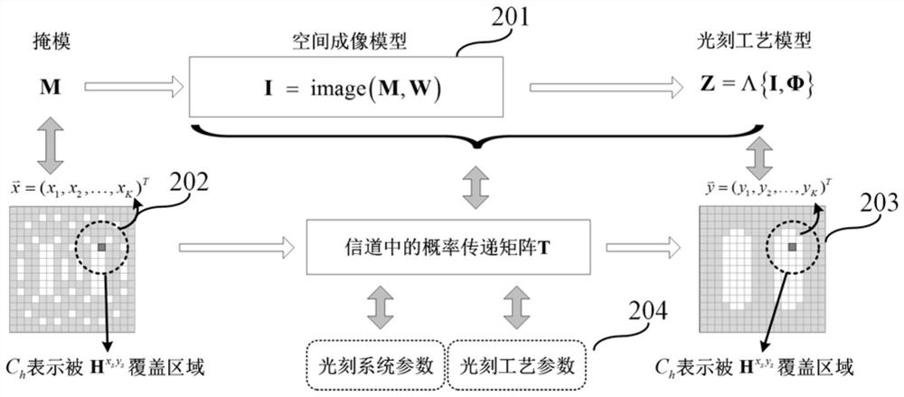
- Informatics computational lithography methods are used to establish a channel model through point diffusion operations, probability distribution construction and mutual information calculations to solve for optimal mask distribution, lithography system parameters and process parameters. Abstract lithography imaging is a channel transmission process and is optimized. Mask pattern to improve imaging accuracy.

A method for optimization of a lithographic process
PatentWO2018077651A1
Innovation
- A method that determines parameter and process window fingerprints to assess uncertainty and probability of performance parameters being outside acceptable ranges, allowing for optimized placement of metrology targets and modification of performance parameter data to enhance yield, incorporating uncertainty and process window metrics for improved control strategies.


Process Variation Impact on Lithography Yield Performance
Process variations represent one of the most critical factors affecting lithography yield performance in advanced semiconductor manufacturing. These variations manifest across multiple dimensions, including mask manufacturing tolerances, photoresist properties, optical system aberrations, and wafer processing conditions. The cumulative impact of these variations creates a complex yield landscape that directly influences the economic viability of computational lithography solutions.
Manufacturing process variations typically follow statistical distributions, with critical dimension uniformity being particularly sensitive to systematic and random fluctuations. Systematic variations often originate from tool-to-tool differences, thermal gradients, and chemical concentration variations across the wafer surface. Random variations, conversely, stem from molecular-level phenomena in photoresist chemistry, shot noise in exposure systems, and stochastic effects during development processes.
The relationship between process variations and yield performance exhibits non-linear characteristics, where small increases in variation can lead to disproportionate yield degradation. This sensitivity becomes more pronounced at advanced technology nodes where design margins continue to shrink. Edge placement errors, line width roughness, and contact hole ellipticity variations directly translate into electrical parameter shifts that can push devices outside specification limits.
Computational lithography optimization must account for these variation sources through robust design methodologies. Monte Carlo simulations incorporating process variation models enable prediction of yield distributions before actual manufacturing. These simulations consider correlated variation sources, such as the relationship between focus variations and resist thickness uniformity, which significantly impact final pattern fidelity.
Advanced process control strategies, including real-time feedback systems and predictive modeling, help mitigate variation impacts on yield performance. Machine learning algorithms increasingly support variation prediction and compensation, enabling proactive adjustments to exposure parameters and optical proximity correction models. The integration of metrology data with computational models creates closed-loop systems that continuously optimize lithography performance against variation-induced yield loss.
Machine Learning Applications in Lithography Yield Prediction
Machine learning has emerged as a transformative technology in computational lithography, offering unprecedented capabilities for yield prediction and optimization. The integration of ML algorithms into lithography processes addresses the growing complexity of advanced semiconductor manufacturing, where traditional rule-based approaches struggle to handle the multidimensional parameter spaces and non-linear relationships inherent in modern lithographic systems.
Deep learning architectures, particularly convolutional neural networks (CNNs), have demonstrated exceptional performance in predicting lithographic outcomes by analyzing mask patterns, process conditions, and wafer characteristics. These models can process vast amounts of historical production data to identify subtle correlations between process parameters and yield metrics that would be impossible to detect through conventional statistical methods.
Supervised learning approaches utilize extensive datasets of process parameters, optical proximity correction (OPC) settings, and corresponding yield results to train predictive models. Random forest algorithms and support vector machines have shown particular effectiveness in handling the high-dimensional feature spaces typical of lithographic processes, while gradient boosting methods excel at capturing complex interactions between variables such as dose, focus, and mask bias.
Unsupervised learning techniques, including clustering algorithms and anomaly detection methods, provide valuable insights into process variations and defect patterns. These approaches can identify previously unknown failure modes and process drift patterns, enabling proactive yield optimization strategies. Principal component analysis and autoencoders have proven effective in dimensionality reduction, helping to isolate the most critical process variables affecting yield outcomes.
Real-time yield prediction systems leverage streaming data from lithography tools, incorporating sensor readings, environmental conditions, and in-line metrology results. These systems employ ensemble methods that combine multiple ML models to provide robust predictions with quantified uncertainty estimates, enabling dynamic process adjustments and preventive maintenance scheduling.
The implementation of reinforcement learning algorithms represents an emerging frontier, where ML agents learn optimal process control strategies through interaction with lithographic systems. These approaches show promise for adaptive process optimization, automatically adjusting parameters in response to changing conditions while maximizing yield objectives and minimizing production costs.
Unlock deeper insights with Patsnap Eureka Quick Research — get a full tech report to explore trends and direct your research. Try now!
Generate Your Research Report Instantly with AI Agent
Supercharge your innovation with Patsnap Eureka AI Agent Platform!