

Comparing Computational Lithography and Direct Write Techniques
APR 24, 20269 MIN READ
Generate Your Research Report Instantly with AI Agent
Patsnap Eureka helps you evaluate technical feasibility & market potential.
Computational Lithography vs Direct Write Background and Goals
Computational lithography and direct write techniques represent two fundamentally different approaches to nanoscale pattern fabrication, each addressing distinct manufacturing challenges in semiconductor and nanotechnology industries. The evolution of these technologies has been driven by the relentless demand for smaller feature sizes, higher precision, and improved manufacturing efficiency across various applications.
Computational lithography emerged as a sophisticated solution to extend the capabilities of traditional optical lithography systems beyond their physical limitations. This approach leverages advanced mathematical algorithms, optical modeling, and computational optimization to enhance pattern fidelity and resolution. The technology encompasses techniques such as optical proximity correction (OPC), source mask optimization (SMO), and inverse lithography technology (ILT), which collectively enable the printing of features significantly smaller than the wavelength of light used in the exposure process.
Direct write techniques, conversely, offer a fundamentally different paradigm by eliminating the need for photomasks entirely. These methods, including electron beam lithography, focused ion beam writing, and laser direct write systems, provide unprecedented flexibility in pattern generation and modification. The technology enables rapid prototyping, small-volume production, and the creation of complex, non-repetitive patterns that would be challenging or economically unfeasible using traditional mask-based approaches.
The primary objective of comparing these technologies centers on understanding their respective strengths, limitations, and optimal application domains. Key evaluation criteria include throughput capabilities, resolution limits, pattern complexity handling, cost structures, and scalability for different production volumes. This analysis aims to provide strategic insights for technology selection based on specific manufacturing requirements and market conditions.
Both technologies continue to evolve rapidly, with computational lithography advancing through machine learning integration and enhanced modeling capabilities, while direct write techniques benefit from improved beam control, higher writing speeds, and novel exposure mechanisms. Understanding their comparative advantages becomes crucial for informed decision-making in advanced manufacturing environments.
The strategic importance of this comparison extends beyond immediate technical considerations to encompass long-term technology roadmaps, investment priorities, and competitive positioning in rapidly evolving markets where precision manufacturing capabilities determine market leadership and innovation potential.
Market Demand for Advanced Lithography Solutions
The global semiconductor industry continues to drive unprecedented demand for advanced lithography solutions as device manufacturers push toward smaller node geometries and more complex architectures. Traditional photolithography approaches face increasing limitations at sub-7nm nodes, creating substantial market opportunities for both computational lithography enhancements and direct write alternatives. The market exhibits strong growth momentum driven by artificial intelligence, high-performance computing, and mobile device requirements demanding higher transistor densities and improved performance characteristics.
Computational lithography solutions represent the largest segment within advanced lithography markets, addressing critical challenges in resolution enhancement, optical proximity correction, and source mask optimization. Major foundries and integrated device manufacturers increasingly rely on sophisticated computational algorithms to extend the capabilities of existing extreme ultraviolet and deep ultraviolet lithography systems. The demand stems from the need to achieve sub-wavelength patterning while maintaining acceptable throughput and cost structures for high-volume manufacturing.
Direct write techniques, including electron beam lithography, focused ion beam systems, and multi-beam approaches, serve specialized market segments requiring ultimate resolution capabilities or rapid prototyping functionality. While traditionally limited by throughput constraints, emerging multi-beam direct write systems address specific applications in photomask manufacturing, research and development, and low-volume specialty device production. The market demand for direct write solutions grows particularly in advanced packaging, MEMS devices, and quantum computing applications where conventional lithography faces fundamental limitations.
The automotive electronics revolution and Internet of Things expansion create additional demand vectors for advanced lithography solutions. These applications require diverse device architectures, specialized materials integration, and cost-effective manufacturing approaches that challenge traditional lithography paradigms. Both computational and direct write techniques find growing applications in power semiconductors, sensor manufacturing, and heterogeneous integration platforms supporting next-generation automotive and industrial systems.
Regional market dynamics show concentrated demand in Asia-Pacific regions, particularly Taiwan, South Korea, and China, where major semiconductor manufacturing capacity resides. North American and European markets focus primarily on equipment development, software solutions, and specialized applications. The geopolitical landscape increasingly influences technology access and development priorities, creating opportunities for domestic lithography solution providers and driving investment in alternative technological approaches across different geographic regions.
Current State and Challenges of Lithography Techniques
Computational lithography has emerged as the dominant paradigm in semiconductor manufacturing, leveraging sophisticated optical proximity correction (OPC), resolution enhancement techniques (RET), and source mask optimization (SMO) to achieve sub-wavelength patterning. Current 193nm immersion lithography systems, combined with multiple patterning techniques such as self-aligned double patterning (SADP) and self-aligned quadruple patterning (SAQP), enable production of 7nm and 5nm node devices. However, these approaches face increasing complexity in mask design, with computational requirements growing exponentially as feature sizes shrink below 10nm.
Extreme ultraviolet (EUV) lithography represents the next frontier in computational lithography, operating at 13.5nm wavelength to enable single-exposure patterning for advanced nodes. Despite significant progress, EUV systems still struggle with power source stability, photoresist sensitivity, and mask defectivity. Current EUV scanners achieve throughput of approximately 185 wafers per hour, falling short of the 200+ wafers per hour required for high-volume manufacturing cost-effectiveness.
Direct write techniques, including electron beam lithography (EBL) and focused ion beam (FIB) systems, offer maskless patterning capabilities with theoretical resolution limits below 5nm. Multi-beam electron lithography systems have demonstrated significant throughput improvements, with companies like IMS Nanofabrication achieving wafer-level patterning speeds approaching 1 wafer per hour for certain applications. However, direct write methods remain constrained by fundamental trade-offs between resolution, throughput, and writing field size.
The primary challenge facing computational lithography lies in the increasing computational burden of OPC and RET algorithms. As design rules tighten, the number of correction iterations required grows substantially, with some advanced node designs requiring over 100 OPC iterations. Machine learning approaches are being integrated to accelerate these computations, but verification and validation of AI-driven corrections remain significant hurdles.
Direct write techniques face distinct challenges centered on throughput limitations and pattern placement accuracy. While EBL can achieve sub-10nm resolution, writing times for full wafer exposure remain prohibitively long for volume production. Stitching errors between writing fields and charging effects in resist materials continue to limit pattern fidelity, particularly for large-area uniform structures.
Both approaches confront materials science challenges, including the development of next-generation photoresists and etch masks capable of supporting increasingly demanding pattern transfer requirements while maintaining acceptable defect densities for yield-sensitive applications.
Existing Computational and Direct Write Solutions
01 Optical Proximity Correction (OPC) and Mask Optimization
Computational lithography techniques employ optical proximity correction algorithms to compensate for diffraction effects and process variations in photolithography. These methods involve iterative optimization of mask patterns to achieve desired wafer patterns, using inverse lithography technology and model-based corrections. Advanced algorithms calculate and adjust mask geometries to account for optical aberrations, ensuring high-fidelity pattern transfer at nanoscale dimensions.- Optical Proximity Correction (OPC) and Mask Optimization: Computational lithography techniques employ optical proximity correction algorithms to compensate for diffraction effects and process variations in photolithography. These methods involve iterative optimization of mask patterns to achieve desired wafer patterns, using inverse lithography technology and model-based corrections. Advanced algorithms calculate and adjust mask geometries to account for optical distortions, improving pattern fidelity and resolution in semiconductor manufacturing.
- Source-Mask Optimization (SMO) and Illumination Control: Source-mask co-optimization techniques simultaneously optimize both the illumination source and mask patterns to enhance lithographic performance. These methods adjust illumination pupil shapes, polarization states, and intensity distributions in conjunction with mask design to maximize process windows and pattern resolution. The optimization process considers the interaction between source characteristics and mask features to achieve optimal imaging results.
- E-beam and Multi-beam Direct Write Systems: Direct write lithography employs electron beam or multiple charged particle beams to directly pattern substrates without using masks. These systems utilize precise beam control, deflection mechanisms, and dose modulation to create nanoscale patterns. Advanced architectures include multi-beam arrays for increased throughput, real-time pattern correction, and adaptive focusing systems to compensate for substrate variations and achieve high-resolution patterning.
- Computational Pattern Generation and Data Processing: Computational methods for pattern data preparation involve fracturing complex design layouts into writing primitives, optimizing exposure sequences, and managing massive data volumes. These techniques include hierarchical data processing, parallel computation algorithms, and efficient data path architectures to handle the computational demands of direct write systems. Pattern preprocessing algorithms optimize beam paths and minimize writing time while maintaining pattern accuracy.
- Dose Correction and Process Calibration: Computational techniques for dose optimization and process calibration ensure uniform pattern exposure across substrates. These methods include proximity effect correction, fogging effect compensation, and loading effect mitigation through computational modeling. Calibration algorithms account for beam blur, substrate charging, and resist response characteristics to achieve accurate critical dimension control and pattern placement in direct write lithography systems.
02 Source-Mask Optimization (SMO) Techniques
Source-mask co-optimization represents an advanced computational approach that simultaneously optimizes both illumination source patterns and mask designs. This technique enhances imaging performance by adjusting pupil configurations and mask patterns in tandem, improving process windows and resolution capabilities. The methodology incorporates mathematical models to balance trade-offs between different lithographic metrics and manufacturing constraints.Expand Specific Solutions03 Electron Beam Direct Write Lithography
Direct write techniques using electron beam technology enable maskless patterning for semiconductor fabrication and nanofabrication applications. These systems provide high-resolution pattern generation through precise beam control and positioning mechanisms. The technology includes multi-beam architectures, dose optimization algorithms, and proximity effect correction methods to achieve accurate pattern placement and dimensional control at the nanometer scale.Expand Specific Solutions04 Machine Learning and AI-Based Lithography Optimization
Artificial intelligence and machine learning algorithms are increasingly applied to computational lithography for pattern prediction, hotspot detection, and process optimization. These approaches utilize neural networks and deep learning models to accelerate mask synthesis, predict lithographic outcomes, and optimize exposure parameters. The methods reduce computational time while maintaining or improving accuracy compared to traditional model-based approaches.Expand Specific Solutions05 Multi-Patterning and Resolution Enhancement Techniques
Advanced computational methods support multiple exposure strategies including double patterning, triple patterning, and self-aligned techniques to extend lithographic capabilities beyond single-exposure limits. These approaches involve pattern decomposition algorithms, color assignment optimization, and overlay error management. The techniques enable continued scaling of semiconductor devices by breaking complex patterns into simpler components that can be manufactured with existing lithography tools.Expand Specific Solutions
Key Players in Lithography Equipment Industry
The computational lithography versus direct write techniques landscape represents a mature semiconductor manufacturing sector experiencing significant technological evolution. The industry operates within a multi-billion dollar market driven by advancing node requirements and emerging applications. Key players demonstrate varying technological maturity levels: established semiconductor giants like Taiwan Semiconductor Manufacturing Co., Intel Corp., and Tokyo Electron Ltd. lead in computational lithography implementation, while specialized firms such as HEIDELBERG INSTRUMENTS Mikrotechnik GmbH, D2S Inc., and Circuit Fabology Microelectronics Equipment Co. focus on direct write innovations. Equipment manufacturers including Applied Materials Inc., Mycronic AB, and Toshiba Corp. bridge both approaches through advanced tooling solutions. Research institutions like Zhejiang University, Naval Research Laboratory, and Commissariat à l'énergie atomique contribute fundamental breakthroughs. The competitive dynamics show computational lithography dominating high-volume production while direct write techniques gain traction in specialized applications, prototyping, and emerging markets requiring flexible, maskless solutions.
Taiwan Semiconductor Manufacturing Co., Ltd.
Technical Solution: TSMC employs advanced computational lithography techniques including optical proximity correction (OPC), source mask optimization (SMO), and inverse lithography technology (ILT) for sub-7nm node manufacturing. Their computational approach uses sophisticated algorithms to predict and compensate for optical effects during photolithography, enabling precise pattern transfer with feature sizes below 5nm. The company integrates machine learning algorithms to optimize mask designs and reduce manufacturing variability, achieving yield rates exceeding 90% for advanced nodes.
Strengths: Industry-leading computational lithography capabilities with proven high-volume manufacturing success. Weaknesses: High computational overhead and significant infrastructure investment requirements for advanced node processing.
Applied Materials, Inc.
Technical Solution: Applied Materials develops both computational lithography solutions and direct write systems including electron beam lithography equipment. Their computational approach focuses on advanced process modeling and correction algorithms integrated with their deposition and etching systems. For direct write applications, they offer electron beam systems capable of sub-10nm resolution for mask making and research applications. The company's holistic approach combines computational optimization with physical process control to achieve precise pattern definition across various substrate materials.
Strengths: Comprehensive equipment portfolio covering both computational and direct write techniques with strong process integration capabilities. Weaknesses: Higher equipment costs and complexity compared to traditional lithography approaches.
Core Innovations in Lithography Pattern Formation
Computational lithography with feature upsizing
PatentActiveUS8793626B2
Innovation
- The method involves identifying marginal feature types through Bossung curves analysis and upsizing these features by 1.5σ in the computational lithography model to re-center parametric data, reducing failures in resistance, capacitance, and drive current by adjusting the reticle design to improve depth of field and focus sensitivity.


Combined E-beam and optical exposure semiconductor lithography
PatentInactiveUS6875624B2
Innovation
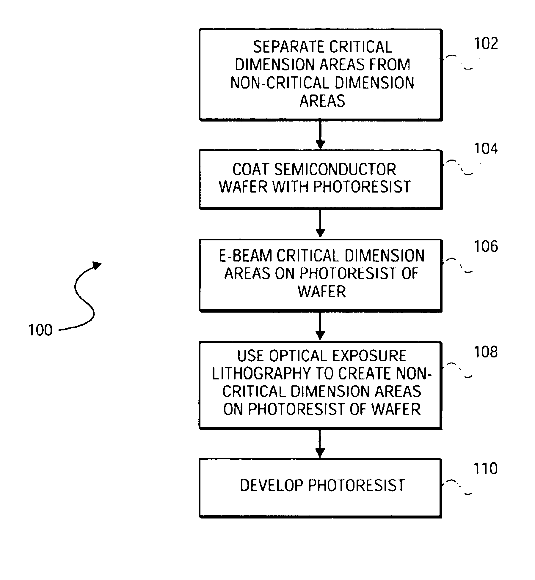
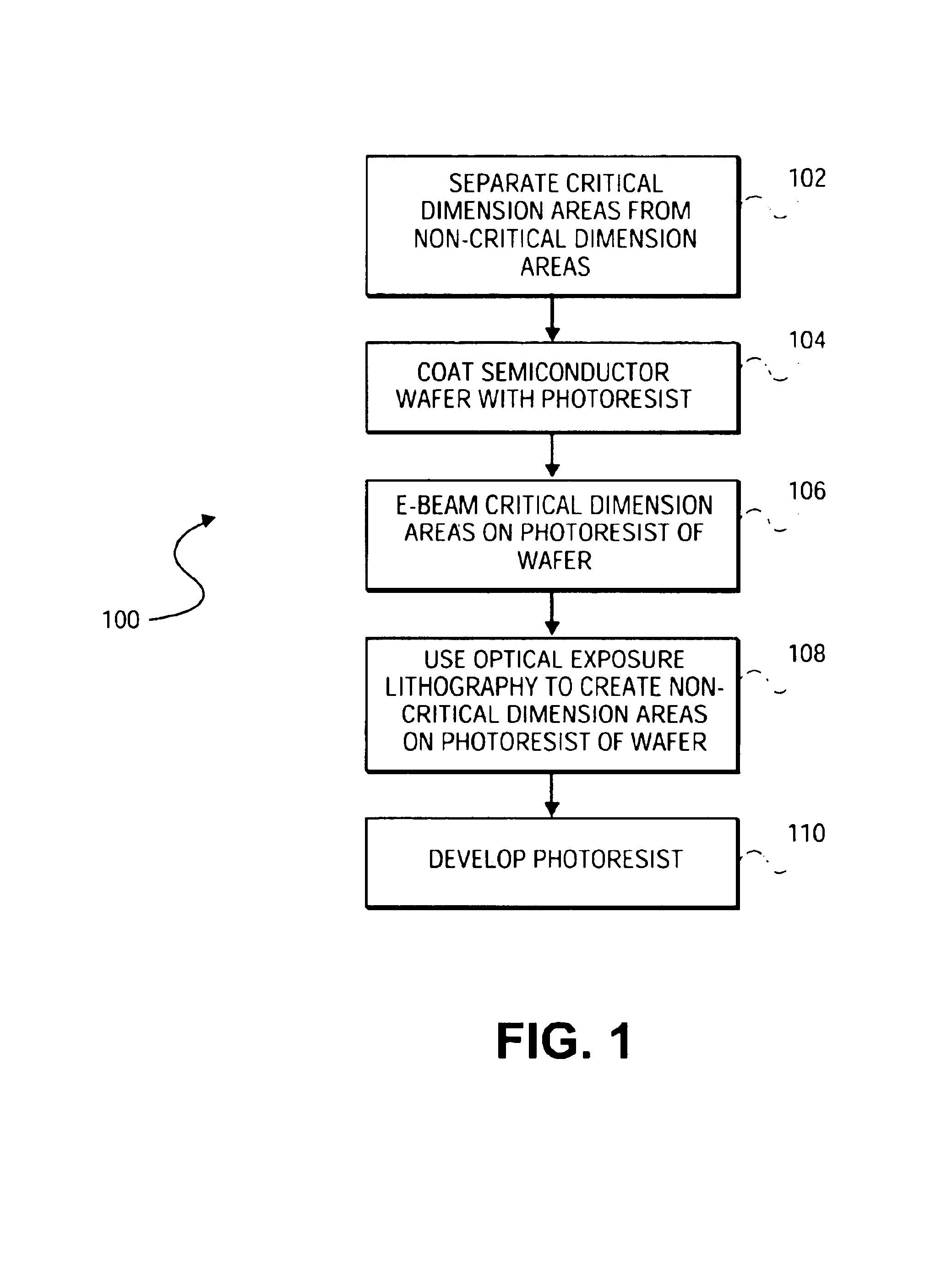
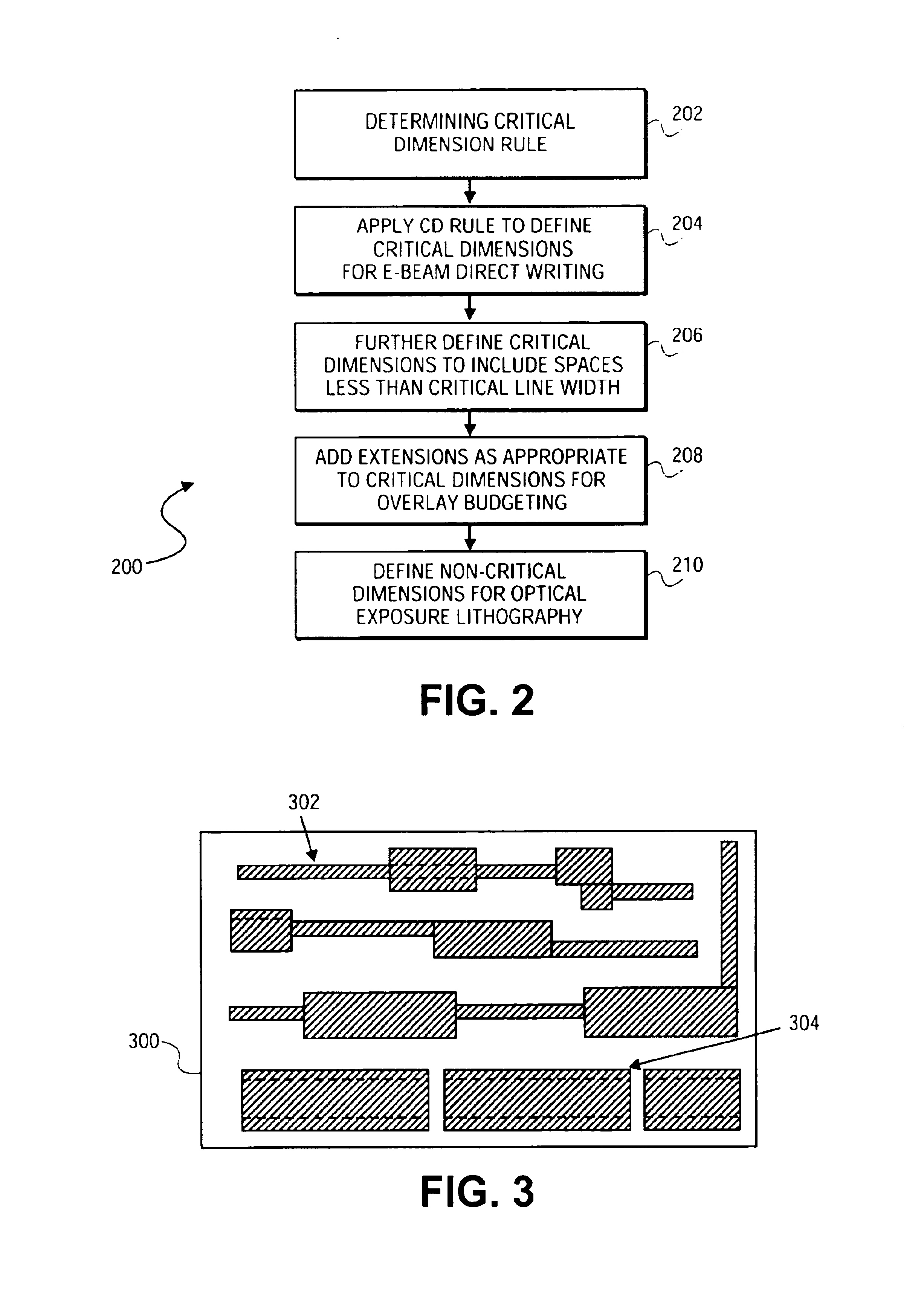
- A combined e-beam and optical exposure lithography method where critical dimension areas are written using precise e-beam direct writing, while non-critical dimension areas are processed with faster optical exposure lithography, separating these areas before transfer to the semiconductor wafer to achieve high resolution and throughput.

Manufacturing Cost and Throughput Analysis
Manufacturing cost analysis reveals significant differences between computational lithography and direct write techniques across multiple economic dimensions. Computational lithography systems require substantial initial capital investments, with advanced EUV lithography tools costing between $150-200 million per unit. However, these systems achieve exceptional throughput rates of 140-170 wafers per hour for high-volume production, resulting in lower per-unit manufacturing costs when amortized across millions of devices. The operational costs include expensive photomasks ranging from $2-5 million for leading-edge nodes, but these masks enable parallel processing of entire wafer surfaces simultaneously.
Direct write techniques present contrasting economic characteristics with lower initial equipment costs typically ranging from $5-20 million per system. Electron beam lithography systems and focused ion beam tools require significantly less capital investment compared to optical lithography infrastructure. However, throughput limitations represent the primary cost challenge, with typical processing rates of 10-50 wafers per hour depending on pattern complexity and resolution requirements. The sequential nature of direct write processes inherently limits production scalability.
Throughput analysis demonstrates computational lithography's superiority in high-volume manufacturing scenarios. Modern immersion lithography systems process complete wafer exposures in 60-90 seconds, enabling annual production capacities exceeding one million wafers per tool. EUV systems, while slower at 3-5 minutes per wafer, still maintain substantial throughput advantages over direct write alternatives. The parallel exposure capability allows simultaneous patterning of hundreds of die per wafer, maximizing manufacturing efficiency.
Direct write techniques exhibit throughput constraints due to their serial processing nature. Electron beam systems require pixel-by-pixel or vector-based pattern generation, with writing times ranging from minutes to hours per die depending on pattern density. Multi-beam electron systems partially address these limitations by employing parallel writing strategies, achieving 10-100x throughput improvements over single-beam configurations, though still falling short of optical lithography rates.
Cost-per-feature analysis favors computational lithography for repetitive patterns and high-volume production, where mask costs distribute across millions of devices. Direct write techniques become economically advantageous for prototyping, low-volume production, and custom applications where mask costs cannot be justified. The crossover point typically occurs at production volumes below 10,000 wafers annually, making direct write techniques particularly suitable for research applications and specialized manufacturing requirements.
Process Integration and Yield Optimization Strategies
Process integration represents a critical differentiator between computational lithography and direct write techniques, fundamentally impacting manufacturing yield and production economics. Computational lithography systems leverage established semiconductor fabrication infrastructure, enabling seamless integration with existing photoresist processing, etching, and metrology workflows. This compatibility allows manufacturers to implement advanced optical proximity correction and source mask optimization without substantial modifications to their production lines.
Direct write techniques, conversely, require specialized process integration approaches due to their unique exposure mechanisms. Electron beam lithography systems necessitate ultra-high vacuum environments and precise substrate handling protocols, while focused ion beam systems demand careful consideration of ion implantation effects on underlying materials. These requirements often mandate dedicated processing modules and modified workflow sequences.
Yield optimization strategies differ significantly between the two approaches. Computational lithography achieves yield enhancement through sophisticated modeling and correction algorithms that predict and compensate for process variations. Machine learning-based dose and focus optimization, combined with advanced mask synthesis techniques, enables consistent pattern fidelity across entire wafers. Statistical process control integration allows real-time adjustment of exposure parameters based on upstream process variations.
Direct write systems optimize yield through different mechanisms, primarily focusing on beam stability, positioning accuracy, and dose uniformity. Advanced beam drift correction algorithms and real-time metrology feedback systems maintain nanometer-level precision throughout extended exposure sequences. Multi-beam architectures distribute exposure tasks to minimize individual beam loading effects and reduce overall processing time.
Defect management strategies also vary considerably. Computational lithography relies on design rule checking and lithography-friendly design practices to prevent systematic defects, while direct write techniques emphasize real-time error detection and correction capabilities. The inherent flexibility of direct write systems allows for adaptive patterning strategies that can compensate for substrate non-uniformities and localized defects during exposure.
Cost-effective yield optimization requires balancing throughput considerations with quality requirements. Computational lithography achieves this through parallel processing of entire fields, while direct write systems increasingly adopt multi-beam architectures and intelligent exposure sequencing to improve productivity while maintaining precision.
Unlock deeper insights with Patsnap Eureka Quick Research — get a full tech report to explore trends and direct your research. Try now!
Generate Your Research Report Instantly with AI Agent
Supercharge your innovation with Patsnap Eureka AI Agent Platform!