

Real-time Predictive Adjustments in Computational Lithography Systems
APR 24, 20269 MIN READ
Generate Your Research Report Instantly with AI Agent
Patsnap Eureka helps you evaluate technical feasibility & market potential.
Computational Lithography Evolution and Predictive Goals
Computational lithography has undergone a remarkable transformation since its inception in the 1980s, evolving from basic optical proximity correction techniques to sophisticated machine learning-driven systems. The early stages focused primarily on geometric corrections to compensate for optical diffraction effects, utilizing rule-based approaches that required extensive manual calibration. As semiconductor feature sizes continued to shrink below the wavelength of exposure light, the complexity of lithographic challenges exponentially increased, necessitating more advanced computational solutions.
The evolution accelerated significantly in the 2000s with the introduction of model-based optical proximity correction and source mask optimization techniques. These developments marked the transition from reactive correction methods to proactive design optimization approaches. The integration of inverse lithography technology further revolutionized the field by enabling the computation of optimal mask patterns directly from desired wafer patterns, fundamentally changing how lithographers approached pattern fidelity challenges.
Recent advances have witnessed the emergence of artificial intelligence and machine learning algorithms in computational lithography workflows. Deep learning models now demonstrate unprecedented capabilities in predicting lithographic outcomes, enabling real-time process adjustments that were previously impossible. The convergence of high-performance computing, advanced algorithms, and comprehensive process modeling has created opportunities for predictive lithography systems that can anticipate and correct potential defects before they occur.
The current technological trajectory points toward fully autonomous lithography systems capable of self-optimization and real-time adaptation. The primary goal of predictive computational lithography is to achieve zero-defect manufacturing through continuous process monitoring and instantaneous corrections. This involves developing algorithms that can process vast amounts of sensor data, predict process variations, and implement corrective actions within the exposure timeframe.
Future predictive goals encompass the development of digital twins for lithography systems, enabling virtual process optimization and predictive maintenance. The integration of edge computing capabilities directly into lithography tools represents another critical objective, allowing for microsecond-level response times to process variations. Additionally, the establishment of comprehensive databases linking process parameters to final outcomes will enable more accurate predictive models and enhanced process control strategies.
Market Demand for Real-time Lithography Process Control
The semiconductor industry faces unprecedented pressure to achieve higher precision and yield in lithography processes as device geometries continue to shrink below 5nm nodes. Traditional lithography systems rely on post-exposure metrology and feedback loops that introduce significant delays, often resulting in entire wafer batches being processed with suboptimal parameters. This reactive approach leads to substantial material waste and reduced manufacturing efficiency, creating urgent demand for real-time process control solutions.
Advanced foundries and memory manufacturers are increasingly seeking computational lithography systems capable of predictive adjustments during exposure processes. The market demand stems from the critical need to minimize overlay errors, critical dimension variations, and focus deviations that can render chips non-functional. Leading semiconductor manufacturers have identified real-time process control as a key enabler for maintaining economic viability in next-generation node production.
The growing complexity of multi-patterning techniques and extreme ultraviolet lithography has amplified the need for instantaneous process corrections. Current market requirements include sub-nanometer overlay accuracy, real-time dose optimization, and dynamic aberration compensation. These demands are driven by the economic reality that even minor process variations can result in significant yield losses, particularly for high-value products such as advanced processors and memory devices.
Market adoption is being accelerated by the increasing cost of advanced lithography equipment and the need to maximize tool utilization. Semiconductor manufacturers are willing to invest in real-time predictive systems that can reduce rework rates and improve first-pass yield. The demand is particularly strong in high-volume manufacturing environments where process stability directly impacts profitability.
The market also shows growing interest in machine learning-enabled predictive algorithms that can anticipate process drift and equipment degradation. This demand reflects the industry's shift toward predictive maintenance and autonomous manufacturing systems. Companies are seeking solutions that integrate seamlessly with existing computational lithography workflows while providing actionable insights for process optimization.
Emerging applications in advanced packaging and heterogeneous integration are creating additional market segments for real-time lithography control. These applications require precise alignment and overlay control across multiple die types and materials, further driving demand for sophisticated real-time adjustment capabilities in computational lithography systems.
Current State of Predictive Adjustment Technologies
The current landscape of predictive adjustment technologies in computational lithography systems represents a convergence of advanced machine learning algorithms, real-time data processing capabilities, and sophisticated optical modeling techniques. Leading semiconductor manufacturers have implemented various approaches to address the growing complexity of sub-7nm node manufacturing requirements, where traditional feed-forward correction methods prove insufficient for maintaining acceptable yield rates.
Machine learning-based predictive models currently dominate the field, with convolutional neural networks and deep learning architectures being extensively deployed for pattern recognition and defect prediction. These systems analyze historical lithography data, wafer inspection results, and process variations to anticipate potential printing errors before they occur. Major foundries report prediction accuracy rates exceeding 85% for critical dimension variations and overlay errors when utilizing ensemble learning approaches.
Real-time data fusion technologies have emerged as a critical enabler, integrating inputs from multiple sensors including interferometric systems, scatterometry tools, and environmental monitoring equipment. Current implementations can process sensor data streams at frequencies up to 1 kHz, enabling sub-second response times for adjustment commands. However, computational bottlenecks remain in complex pattern areas where full-chip simulation requirements exceed available processing capacity.
Adaptive optical correction systems represent another significant advancement, utilizing deformable mirrors and programmable illumination sources to implement predictive adjustments. These systems can modify exposure conditions dynamically based on predicted process variations, achieving correction ranges of ±20nm for critical dimensions and ±5nm for overlay accuracy. Integration with existing scanner architectures remains challenging due to hardware limitations and thermal stability requirements.
Current predictive algorithms primarily focus on systematic error patterns, with limited capability for addressing stochastic variations that become increasingly prominent at advanced nodes. Edge placement error prediction has shown particular promise, with some implementations achieving 70% reduction in post-lithography correction requirements. However, computational complexity scales exponentially with pattern density, limiting real-time application to selected critical layers.
The integration of physics-based models with data-driven approaches represents the current state-of-the-art, combining rigorous optical simulations with empirical learning from production data. This hybrid methodology addresses both known physical phenomena and unexpected process interactions, though calibration requirements remain substantial for new product introductions.
Existing Real-time Prediction and Adjustment Solutions
01 Machine learning-based predictive modeling for lithography process optimization
Advanced computational systems utilize machine learning algorithms and neural networks to predict lithography outcomes and make real-time adjustments. These systems analyze historical process data, pattern characteristics, and environmental variables to build predictive models that can anticipate defects or deviations before they occur. The models continuously learn from new data to improve prediction accuracy and enable proactive process control.- Machine learning-based predictive modeling for lithography process optimization: Advanced computational systems utilize machine learning algorithms and artificial intelligence to predict lithography outcomes and make real-time adjustments. These systems analyze historical process data, pattern characteristics, and manufacturing parameters to build predictive models that can anticipate defects or deviations before they occur. The models continuously learn from new data to improve prediction accuracy and enable proactive process control, reducing the need for post-exposure corrections and improving overall manufacturing efficiency.
- Real-time optical proximity correction and mask optimization: Computational lithography systems employ dynamic optical proximity correction techniques that adjust in real-time based on measured process variations and substrate conditions. These systems continuously monitor exposure parameters and automatically modify mask patterns or illumination settings to compensate for systematic and random variations. The real-time adjustment capability ensures consistent pattern fidelity across different process conditions and substrate locations, maintaining critical dimension uniformity throughout the manufacturing process.
- Adaptive dose and focus control systems: Advanced lithography platforms incorporate predictive algorithms that dynamically adjust exposure dose and focus parameters based on real-time metrology feedback and computational models. These systems predict optimal exposure conditions for each die or field by analyzing substrate topography, reflectivity variations, and previous exposure results. The adaptive control mechanisms enable compensation for wafer-level variations and process drift, ensuring consistent lithographic performance across entire production lots.
- Source-mask co-optimization with predictive feedback: Computational systems integrate source-mask co-optimization techniques with real-time predictive capabilities to simultaneously optimize illumination source shapes and mask patterns. These systems use advanced algorithms to predict the combined effect of source and mask modifications on final wafer patterns, enabling rapid convergence to optimal solutions. The predictive feedback loop allows for continuous refinement of both source and mask designs based on actual manufacturing results, improving process window and pattern fidelity.
- Multi-variable process monitoring and predictive maintenance: Integrated computational systems monitor multiple lithography process variables simultaneously and use predictive analytics to forecast equipment performance degradation and process excursions. These systems collect data from various sensors and metrology tools, applying statistical analysis and pattern recognition to identify trends that precede quality issues. The predictive capabilities enable preemptive adjustments to process parameters or scheduling of maintenance activities before defects occur, maximizing equipment uptime and yield.
02 Real-time feedback control systems with sensor integration
Computational lithography systems incorporate multiple sensors and metrology tools that provide real-time feedback during the exposure process. These systems collect data on parameters such as dose, focus, overlay, and environmental conditions, then use computational algorithms to make immediate adjustments to compensate for variations. The feedback loop operates at high speed to maintain process stability and ensure pattern fidelity throughout production runs.Expand Specific Solutions03 Adaptive optical proximity correction with dynamic pattern adjustment
Systems employ computational methods to perform optical proximity correction that adapts in real-time based on measured or predicted process conditions. The technology analyzes the interaction between mask patterns and lithography processes, then dynamically modifies correction parameters to account for variations in resist properties, illumination conditions, or substrate characteristics. This enables maintenance of critical dimension uniformity across different process windows.Expand Specific Solutions04 Predictive maintenance and process drift compensation
Computational systems monitor equipment performance parameters and process trends to predict when maintenance is needed or when process drift is occurring. By analyzing patterns in historical data and current measurements, these systems can forecast equipment degradation, consumable depletion, or environmental changes that affect lithography results. Predictive adjustments are made to process recipes or equipment settings to compensate for anticipated changes before they impact product quality.Expand Specific Solutions05 Multi-variable optimization algorithms for process window enhancement
Advanced computational approaches use multi-variable optimization algorithms to simultaneously adjust multiple lithography parameters in real-time. These systems evaluate complex interactions between dose, focus, illumination settings, and mask bias to maximize the process window and minimize defect probability. The algorithms can rapidly explore parameter space and identify optimal settings that adapt to changing conditions or different pattern types within a single exposure field.Expand Specific Solutions
Key Players in Semiconductor Lithography Industry
The real-time predictive adjustments in computational lithography systems market represents a mature, high-stakes segment within the semiconductor manufacturing ecosystem. The industry has reached an advanced consolidation phase, dominated by established players like ASML Netherlands BV, which maintains market leadership in EUV lithography systems, and Canon Inc., providing alternative lithography solutions. The market demonstrates significant scale, driven by increasing demand for advanced node semiconductors and AI-driven manufacturing optimization. Technology maturity varies across the competitive landscape, with companies like Applied Materials, Cadence Design Systems, and Mentor Graphics delivering sophisticated computational solutions, while emerging players such as Dongfang Jingyuan Electron and Shanghai Microelectronics Equipment represent growing regional capabilities. The sector benefits from substantial R&D investments from foundries like GLOBALFOUNDRIES and Shanghai Huali Microelectronics, alongside specialized software providers like D2S and Silvaco, creating a robust ecosystem supporting next-generation predictive lithography technologies.
ASML Netherlands BV
Technical Solution: ASML has developed advanced computational lithography systems that integrate real-time predictive adjustments through their proprietary holistic lithography approach. Their systems utilize machine learning algorithms and advanced optical proximity correction (OPC) techniques to predict and compensate for process variations in real-time during exposure. The technology incorporates dose and focus control systems that can make sub-nanometer adjustments based on predictive models that analyze wafer topography, resist properties, and environmental conditions. Their latest EUV lithography systems feature integrated metrology and computational engines that enable continuous process optimization and real-time error correction, significantly improving yield and pattern fidelity for advanced semiconductor manufacturing nodes.
Strengths: Market leader in advanced lithography with comprehensive real-time adjustment capabilities and integrated EUV technology. Weaknesses: High system cost and complexity, requiring significant infrastructure investment and specialized expertise.
Applied Materials, Inc.
Technical Solution: Applied Materials has developed computational lithography solutions that incorporate real-time predictive adjustments through their Centura platform and advanced process control systems. Their approach combines in-situ metrology with predictive modeling algorithms to enable real-time dose and focus corrections during the lithography process. The system utilizes advanced sensors and feedback control mechanisms that can predict process deviations and automatically adjust exposure parameters to maintain critical dimension uniformity and overlay accuracy. Their technology integrates machine learning models that continuously learn from process data to improve prediction accuracy and reduce cycle times while maintaining high throughput manufacturing requirements.
Strengths: Strong integration capabilities with comprehensive semiconductor manufacturing equipment portfolio and proven process control expertise. Weaknesses: Limited to specific equipment platforms and may require extensive system integration for full implementation.
Core Algorithms for Predictive Lithography Control
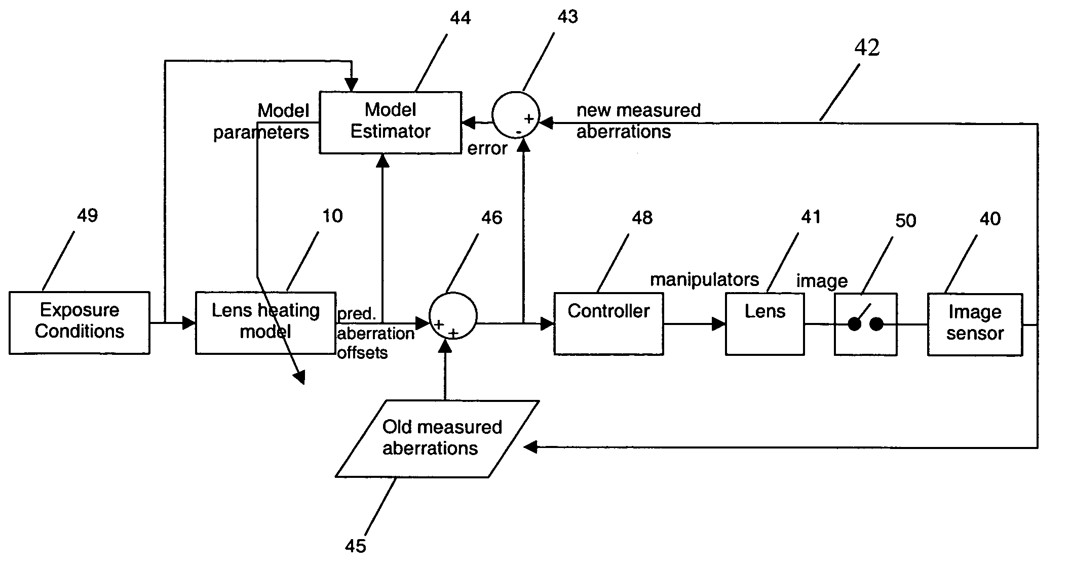
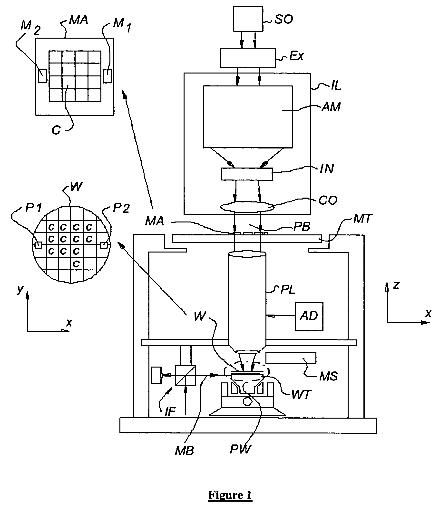
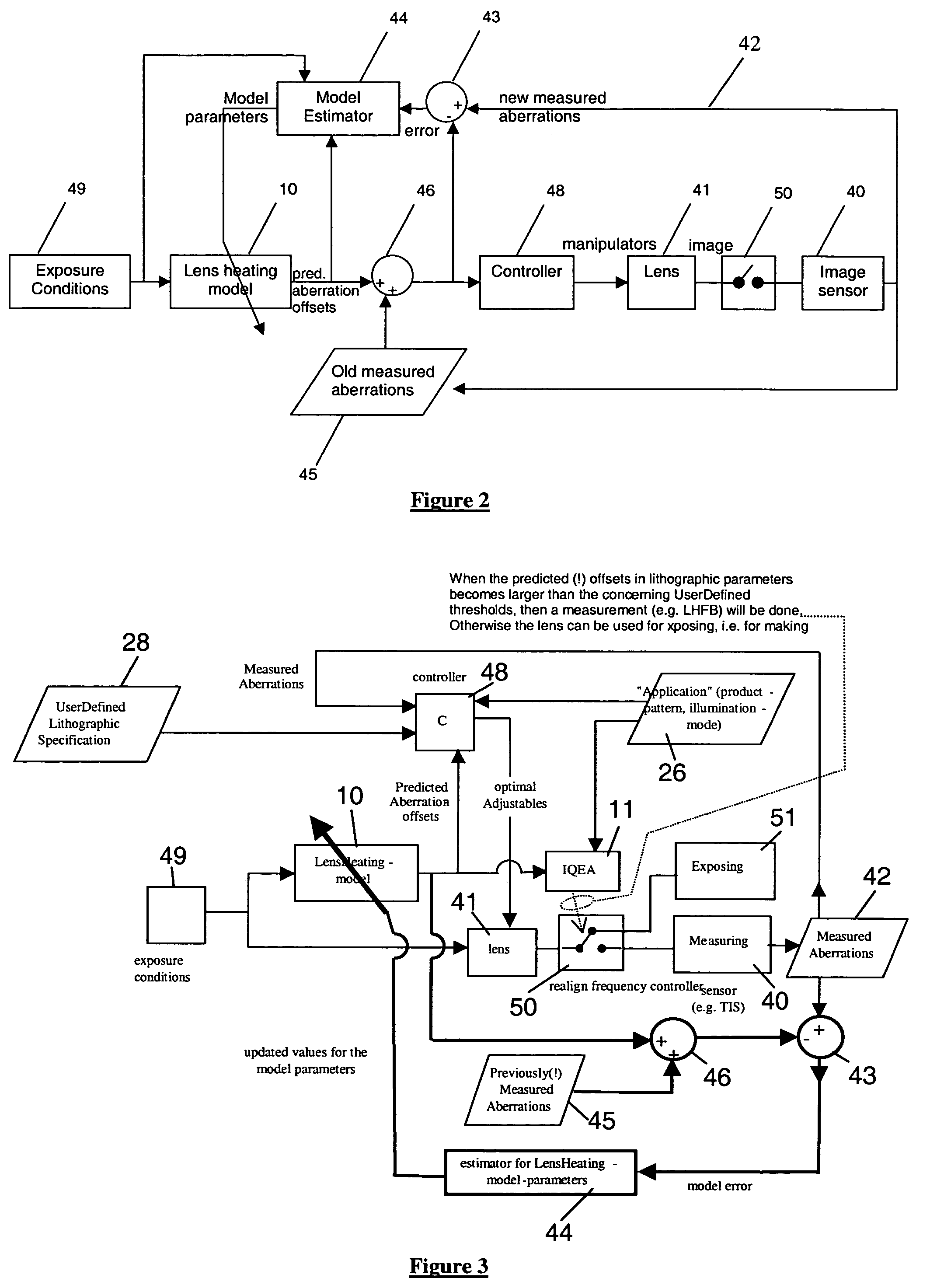
Lithographic projection apparatus and a device manufacturing method using such lithographic projection apparatus
PatentInactiveUS20080252870A1
Innovation
- A predictive system within the lithographic projection apparatus that models and compensates for lens aberrations using a lens heating model, adjusting image parameters and optical settings to optimize image quality for specific applications by generating application-specific control signals to correct for aberrations based on measured values.


Lithographic projection apparatus and device manufacturing method using such lithographic projection apparatus
PatentInactiveUS7262831B2
Innovation
- The implementation of a predictive control system that measures and compensates for projection system aberrations using a measurement system, predictive control, and inline model identification to maintain aberration corrections within acceptable performance criteria, allowing for real-time adjustments and optimized image quality.

Machine Learning Integration in Lithography Workflows
Machine learning integration represents a transformative paradigm shift in computational lithography workflows, fundamentally altering how semiconductor manufacturing processes approach pattern fidelity and process optimization. The convergence of artificial intelligence algorithms with traditional lithographic systems has created unprecedented opportunities for enhancing manufacturing precision while reducing computational overhead traditionally associated with complex optical proximity correction and resolution enhancement techniques.
Deep learning architectures, particularly convolutional neural networks and transformer-based models, have demonstrated remarkable capabilities in pattern recognition and prediction tasks within lithographic contexts. These algorithms excel at identifying subtle correlations between mask designs, process parameters, and final wafer outcomes that conventional rule-based systems often overlook. The integration enables real-time analysis of vast datasets encompassing exposure conditions, resist chemistry variations, and environmental factors that influence pattern transfer accuracy.
Reinforcement learning frameworks have emerged as particularly promising approaches for optimizing lithographic workflows through continuous learning and adaptation. These systems can dynamically adjust process parameters based on feedback from previous exposures, creating self-improving manufacturing environments that enhance yield and reduce defect rates over time. The ability to learn from both successful and failed exposures provides valuable insights for process refinement.
Neural network-based optical proximity correction models have revolutionized mask design optimization by replacing computationally intensive physics-based simulations with rapid inference engines. These models can predict pattern distortions and recommend corrective measures in milliseconds rather than hours, enabling real-time design rule checking and mask optimization during the design phase.
The integration of machine learning extends beyond individual process steps to encompass holistic workflow optimization, where algorithms coordinate multiple lithographic tools and processes simultaneously. This system-level approach enables predictive maintenance, adaptive process control, and intelligent resource allocation across entire fabrication facilities, maximizing throughput while maintaining quality standards.
However, successful implementation requires careful consideration of model training data quality, algorithm interpretability, and integration with existing manufacturing execution systems to ensure seamless adoption within established production environments.
Economic Impact of Real-time Lithography Optimization
The implementation of real-time predictive adjustments in computational lithography systems represents a paradigm shift that delivers substantial economic benefits across the semiconductor manufacturing ecosystem. The primary economic driver stems from the dramatic reduction in defect rates and rework cycles, which traditionally account for 15-25% of total production costs in advanced node manufacturing. Real-time optimization enables immediate correction of lithographic errors before they propagate through subsequent processing steps, eliminating the need for costly wafer scrapping and reprocessing.
Manufacturing efficiency gains translate directly into improved fab utilization rates and throughput optimization. Traditional lithography processes require extensive offline metrology and feedback loops that can delay production by 6-12 hours per lot. Real-time systems compress this feedback cycle to minutes, enabling continuous production flow and reducing work-in-progress inventory costs. This acceleration in cycle time allows fabs to increase their effective capacity by 8-15% without additional capital equipment investment.
The technology's impact on yield enhancement creates compounding economic benefits, particularly for advanced nodes where each percentage point of yield improvement can represent millions of dollars in revenue per quarter. Real-time predictive adjustments enable consistent achievement of target critical dimensions and overlay specifications, reducing yield loss from lithographic sources by 40-60% compared to conventional feed-forward control systems.
Capital efficiency improvements emerge from extended equipment lifetime and reduced maintenance requirements. Predictive algorithms optimize exposure conditions to minimize stress on optical components and reduce the frequency of costly lens replacements and system recalibrations. This optimization can extend major maintenance intervals by 20-30%, significantly reducing both direct maintenance costs and production downtime.
The competitive advantage gained through faster time-to-market for new process nodes creates substantial revenue opportunities. Fabs implementing real-time lithography optimization can achieve production readiness 3-6 months earlier than competitors using traditional approaches, capturing premium pricing during the initial market introduction phase. This first-mover advantage is particularly valuable in high-volume consumer electronics markets where early production capability commands significant price premiums.
Unlock deeper insights with Patsnap Eureka Quick Research — get a full tech report to explore trends and direct your research. Try now!
Generate Your Research Report Instantly with AI Agent
Supercharge your innovation with Patsnap Eureka AI Agent Platform!