

Comparing Computational Lithography and Optical Proximity Correction
APR 24, 202610 MIN READ
Generate Your Research Report Instantly with AI Agent
Patsnap Eureka helps you evaluate technical feasibility & market potential.
Computational Lithography and OPC Background and Objectives
Computational lithography represents a paradigm shift in semiconductor manufacturing, emerging from the fundamental limitations of traditional optical lithography systems. As semiconductor devices continue to scale down according to Moore's Law, the wavelength of light used in photolithography has remained relatively constant, creating a significant challenge where feature sizes approach or exceed the diffraction limits of the optical systems. This technological evolution has necessitated the development of sophisticated computational methods to bridge the gap between optical capabilities and manufacturing requirements.
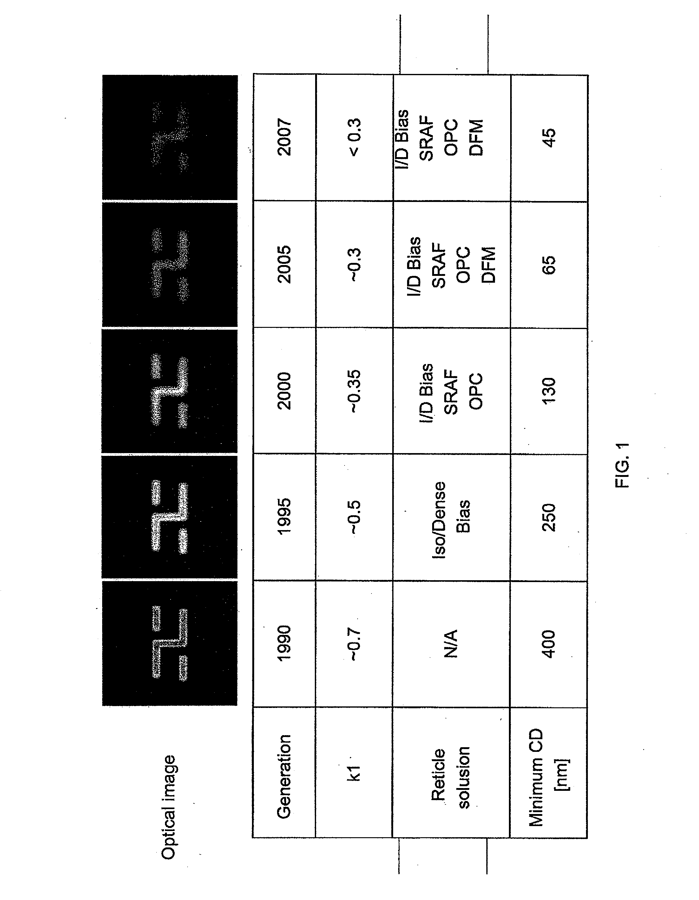
The historical development of computational lithography can be traced back to the early 2000s when the semiconductor industry first encountered serious resolution limitations with 193nm ArF lithography. Traditional approaches relied primarily on hardware improvements and resist chemistry optimization, but these methods proved insufficient for sub-100nm manufacturing nodes. The industry recognized that computational approaches would be essential to extend optical lithography beyond its natural limits, leading to the emergence of resolution enhancement techniques and model-based corrections.
Optical Proximity Correction emerged as one of the earliest and most successful computational lithography techniques, initially developed to address systematic pattern distortions caused by optical diffraction effects. OPC fundamentally changed the approach to mask design by introducing intentional pre-distortions to compensate for predictable optical and process effects. This technique evolved from simple rule-based corrections to sophisticated model-based approaches that could handle increasingly complex geometries and process variations.
The primary objective of computational lithography extends beyond simple pattern correction to encompass comprehensive optimization of the entire lithographic process. Modern computational lithography aims to simultaneously optimize mask patterns, illumination conditions, and process parameters to achieve maximum manufacturing yield and pattern fidelity. This holistic approach represents a significant departure from traditional sequential optimization methods, enabling more aggressive scaling and improved process robustness.
Current technological objectives focus on enabling cost-effective manufacturing at advanced nodes while maintaining acceptable defect rates and cycle times. The industry seeks to extend 193nm immersion lithography through multiple patterning techniques combined with advanced computational methods, delaying the need for expensive next-generation lithography technologies. Additionally, computational lithography aims to improve design-manufacturing co-optimization, enabling better communication between design and manufacturing teams through shared computational models and constraints.
The evolution toward inverse lithography and source-mask optimization represents the cutting edge of computational lithography development. These techniques abandon traditional design rule constraints in favor of physics-based optimization algorithms that can discover non-intuitive solutions to complex patterning challenges. The ultimate goal involves creating fully automated design-to-manufacturing flows that can handle arbitrary target patterns while optimizing for multiple objectives including resolution, process window, and manufacturing cost.
Market Demand for Advanced Lithography Solutions
The semiconductor industry's relentless pursuit of smaller node technologies has created an unprecedented demand for advanced lithography solutions, particularly computational lithography and optical proximity correction technologies. As chip manufacturers push toward sub-3nm processes, traditional lithography approaches face fundamental physical limitations that can only be overcome through sophisticated computational methods.
The market demand stems primarily from the exponential increase in design complexity at advanced nodes. Modern semiconductor devices require precise pattern fidelity across billions of transistors, where even nanometer-scale deviations can result in yield loss or performance degradation. This precision requirement has transformed lithography from a purely optical process into a computationally intensive discipline where mathematical modeling and correction algorithms are essential.
Leading foundries and integrated device manufacturers represent the primary demand drivers for these technologies. These companies face mounting pressure to maintain Moore's Law progression while managing escalating manufacturing costs. The economic imperative is clear: without advanced computational lithography and OPC solutions, the yield rates at cutting-edge nodes would be commercially unviable, potentially rendering entire technology generations economically unfeasible.
The automotive and mobile device sectors have emerged as significant demand catalysts. Advanced driver assistance systems, artificial intelligence processors, and high-performance mobile chipsets require the density and performance benefits that only leading-edge nodes can provide. This application-driven demand creates a cascading effect throughout the semiconductor supply chain, intensifying the need for more sophisticated lithography solutions.
Memory manufacturers constitute another critical demand segment. As data storage requirements continue expanding exponentially, memory devices must achieve higher densities while maintaining reliability. Three-dimensional NAND flash and advanced DRAM architectures rely heavily on computational lithography techniques to achieve the precise vertical and horizontal pattern control necessary for multi-layer structures.
The emergence of specialized computing architectures, including quantum processors and neuromorphic chips, has introduced new lithography challenges that traditional approaches cannot address. These applications often require unconventional pattern geometries and material combinations, driving demand for more flexible and adaptive computational lithography solutions.
Market dynamics also reflect the consolidation of lithography equipment suppliers and the increasing specialization of software providers. The high barriers to entry in this field have created a concentrated supplier base, while the growing complexity of computational requirements has spawned specialized software companies focused exclusively on lithography modeling and correction algorithms.
Current State and Challenges in Computational Lithography
Computational lithography has emerged as a critical enabler for advanced semiconductor manufacturing, particularly as feature sizes continue to shrink below the wavelength of exposure light. The field encompasses various techniques including Optical Proximity Correction (OPC), Source Mask Optimization (SMO), and inverse lithography technology, all aimed at achieving precise pattern transfer on silicon wafers. Current implementations leverage sophisticated algorithms and high-performance computing resources to predict and compensate for optical and process-induced distortions.
The technology landscape is dominated by established Electronic Design Automation (EDA) companies such as Synopsys, Cadence, and Mentor Graphics, which provide comprehensive computational lithography solutions. These platforms integrate complex physical models that account for optical diffraction, photoresist chemistry, and etching processes. Advanced nodes below 7nm require increasingly sophisticated correction algorithms, with some solutions incorporating machine learning techniques to improve accuracy and reduce computational overhead.
Despite significant progress, several fundamental challenges persist in computational lithography implementation. Computational complexity remains a primary bottleneck, as full-chip OPC processing can require weeks of runtime even on high-performance computing clusters. The exponential increase in correction complexity with shrinking feature sizes creates scalability issues that directly impact time-to-market for new semiconductor products. Memory requirements for storing and processing massive layout databases often exceed available system resources, necessitating complex data management strategies.
Model accuracy represents another critical challenge, particularly for emerging materials and process technologies. Current resist models struggle to accurately predict three-dimensional effects and stochastic variations that become increasingly significant at advanced nodes. The gap between simulated and actual wafer results often requires extensive calibration cycles, consuming valuable development time and resources. Process window optimization across multiple patterning steps adds additional complexity layers that existing tools handle with varying degrees of success.
Manufacturing variability introduces further complications, as computational lithography models must account for equipment-specific characteristics and process drift over time. The integration of multiple patterning techniques, such as self-aligned double patterning and extreme ultraviolet lithography, requires sophisticated co-optimization approaches that current solutions address incompletely. Edge placement error control becomes increasingly challenging as design rules tighten, demanding higher precision from correction algorithms while maintaining reasonable computational requirements.
Current OPC and Computational Lithography Solutions
01 Model-based optical proximity correction methods
Computational lithography techniques employ model-based approaches to predict and correct optical proximity effects. These methods utilize mathematical models that simulate the optical imaging process, including diffraction and interference effects. The models calculate how light interacts with mask patterns and predict the resulting wafer patterns. By comparing simulated results with desired patterns, corrections can be applied to mask geometries to compensate for optical distortions. This approach enables accurate prediction of pattern fidelity and systematic correction of proximity effects across various feature sizes and densities.- Model-based optical proximity correction methods: Computational lithography techniques employ model-based approaches to predict and correct optical proximity effects. These methods utilize mathematical models that simulate the optical imaging process, including diffraction and interference effects, to predict how patterns will be printed on wafers. The models are calibrated using empirical data and then used to modify mask patterns systematically to compensate for proximity effects. Iterative optimization algorithms adjust feature edges and add sub-resolution assist features to achieve desired printed patterns with high fidelity.
- Rule-based optical proximity correction techniques: Rule-based correction approaches apply predefined correction rules derived from empirical observations and test pattern results. These techniques use lookup tables and geometric rules to determine how much to adjust feature dimensions based on their local environment and neighboring pattern density. The corrections are typically applied based on pattern classification and edge placement requirements. This approach offers faster computation times compared to full model-based methods while still providing effective correction for many common lithographic situations.
- Sub-resolution assist feature placement: Computational methods are used to determine optimal placement of sub-resolution assist features that improve pattern fidelity without being printed themselves. These features are strategically positioned near main pattern features to manipulate the aerial image intensity distribution and improve depth of focus and process window. Algorithms analyze the local pattern environment and apply optimization techniques to determine the size, shape, and position of assist features. The placement considers manufacturing constraints and ensures the assist features remain below the resolution threshold of the lithography system.
- Machine learning and inverse lithography techniques: Advanced computational approaches employ machine learning algorithms and inverse problem solving to optimize mask patterns. These techniques work backwards from desired wafer patterns to determine optimal mask configurations. Neural networks and other learning algorithms can be trained on large datasets to predict optimal corrections more efficiently. Inverse lithography formulates the mask optimization as an inverse problem where the target is the desired wafer pattern and the solution is the mask pattern that produces it. These methods can explore larger solution spaces and potentially find more optimal corrections than traditional forward-modeling approaches.
- Process window optimization and verification: Computational lithography includes methods for optimizing and verifying the process window of corrected mask patterns. These techniques evaluate pattern performance across ranges of focus and exposure conditions to ensure robust manufacturing. Algorithms assess critical dimension variation, pattern fidelity, and defect probability across the process window. Optimization methods adjust corrections to maximize the usable process window while meeting all design requirements. Verification tools simulate the lithographic process under various conditions to identify potential weak points and ensure manufacturability before mask fabrication.
02 Rule-based optical proximity correction techniques
Rule-based correction methods apply predetermined correction rules derived from empirical data and experimental observations. These techniques utilize lookup tables and correction recipes that specify how to modify mask features based on their geometric characteristics and surrounding pattern context. The rules are typically developed through extensive characterization of lithographic processes and define corrections for specific feature types, dimensions, and proximity conditions. This approach offers computational efficiency and can be rapidly applied to large design layouts, making it suitable for production environments where processing speed is critical.Expand Specific Solutions03 Machine learning and artificial intelligence in OPC
Advanced computational methods incorporate machine learning algorithms and artificial intelligence techniques to enhance optical proximity correction. These approaches train neural networks or other learning models on extensive datasets of mask patterns and their corresponding wafer results. The trained models can predict lithographic outcomes and generate corrections more efficiently than traditional methods. Deep learning techniques enable pattern recognition and classification of complex geometric configurations, allowing for adaptive correction strategies that improve with accumulated data. This methodology reduces computational time while maintaining or improving correction accuracy.Expand Specific Solutions04 Inverse lithography technology and mask optimization
Inverse lithography approaches work backward from desired wafer patterns to determine optimal mask configurations. These techniques formulate the mask design problem as an optimization task, where algorithms iteratively adjust mask patterns to minimize differences between simulated and target wafer images. The methods consider the full optical system characteristics and can generate non-intuitive mask shapes that produce superior wafer results. Optimization algorithms may employ gradient-based methods, genetic algorithms, or other computational techniques to explore the solution space and converge on optimal or near-optimal mask designs.Expand Specific Solutions05 Sub-resolution assist features and advanced mask enhancement
Computational lithography enables the strategic placement of sub-resolution assist features that improve pattern fidelity without printing on the wafer. These techniques analyze the optical environment around main features and determine optimal locations and dimensions for assist geometries. The assist features modify the aerial image to enhance contrast, improve depth of focus, and reduce proximity effects for critical patterns. Advanced algorithms automatically generate and optimize these enhancement features based on process window requirements and manufacturing constraints, ensuring robust lithographic performance across process variations.Expand Specific Solutions
Key Players in EDA and Semiconductor Manufacturing
The computational lithography and optical proximity correction market represents a mature yet rapidly evolving sector within the semiconductor industry, driven by the relentless push toward smaller process nodes and increasing design complexity. The market demonstrates substantial growth potential as foundries like TSMC, Samsung Electronics, SMIC, GlobalFoundries, and UMC require increasingly sophisticated lithography solutions to maintain manufacturing precision at advanced nodes. Technology maturity varies significantly across market segments, with established EDA leaders like Cadence Design Systems, Siemens Industry Software, and Mentor Graphics offering comprehensive OPC solutions, while specialized firms such as D2S and Silvaco focus on next-generation computational lithography innovations. Equipment manufacturers including ASML Netherlands and Applied Materials drive hardware advancement, while emerging players like Moyan Computing Science represent growing regional capabilities, particularly in Asia-Pacific markets where foundry expansion continues accelerating.
Siemens Industry Software, Inc.
Technical Solution: Siemens provides computational lithography solutions through their Calibre platform, featuring advanced optical proximity correction and computational lithography capabilities. Their technology incorporates physics-based modeling with empirical corrections to achieve high accuracy in pattern prediction and correction. The platform supports both traditional OPC and inverse lithography approaches, with particular strength in handling complex 3D mask effects and process variations. Siemens' solution includes advanced curvilinear OPC capabilities and supports multi-patterning techniques essential for sub-10nm manufacturing processes, with integrated design rule checking and verification workflows.
Strengths: Mature platform with extensive industry adoption, robust 3D modeling capabilities, comprehensive verification integration. Weaknesses: Computational intensity for advanced curvilinear corrections, requires significant expertise for optimal configuration.
Cadence Design Systems, Inc.
Technical Solution: Cadence offers comprehensive computational lithography solutions through their Litho Physical Verification platform, which includes advanced optical proximity correction capabilities. Their technology employs machine learning-enhanced OPC algorithms that can reduce mask complexity by up to 30% while maintaining pattern fidelity requirements. The platform integrates inverse lithography technology (ILT) with traditional rule-based and model-based OPC approaches, enabling optimization for complex 2D patterns at advanced nodes. Cadence's solution supports full-chip computational lithography workflows with distributed computing capabilities for handling large-scale designs efficiently.
Strengths: Comprehensive EDA ecosystem integration, advanced machine learning algorithms, scalable distributed computing architecture. Weaknesses: Requires extensive calibration for new process nodes, high licensing costs for full feature sets.
Core Innovations in Resolution Enhancement Techniques
Parallel mask rule checking on evolving mask shapes in optical proximity correction flows
PatentActiveUS20230289509A1
Innovation
- The implementation of parallel mask rule checking systems that adjust multiple edges simultaneously, utilizing a tree structure to share information and minimize geometric area changes, thereby reducing traversal bias and promoting symmetry in mask shape adjustments.


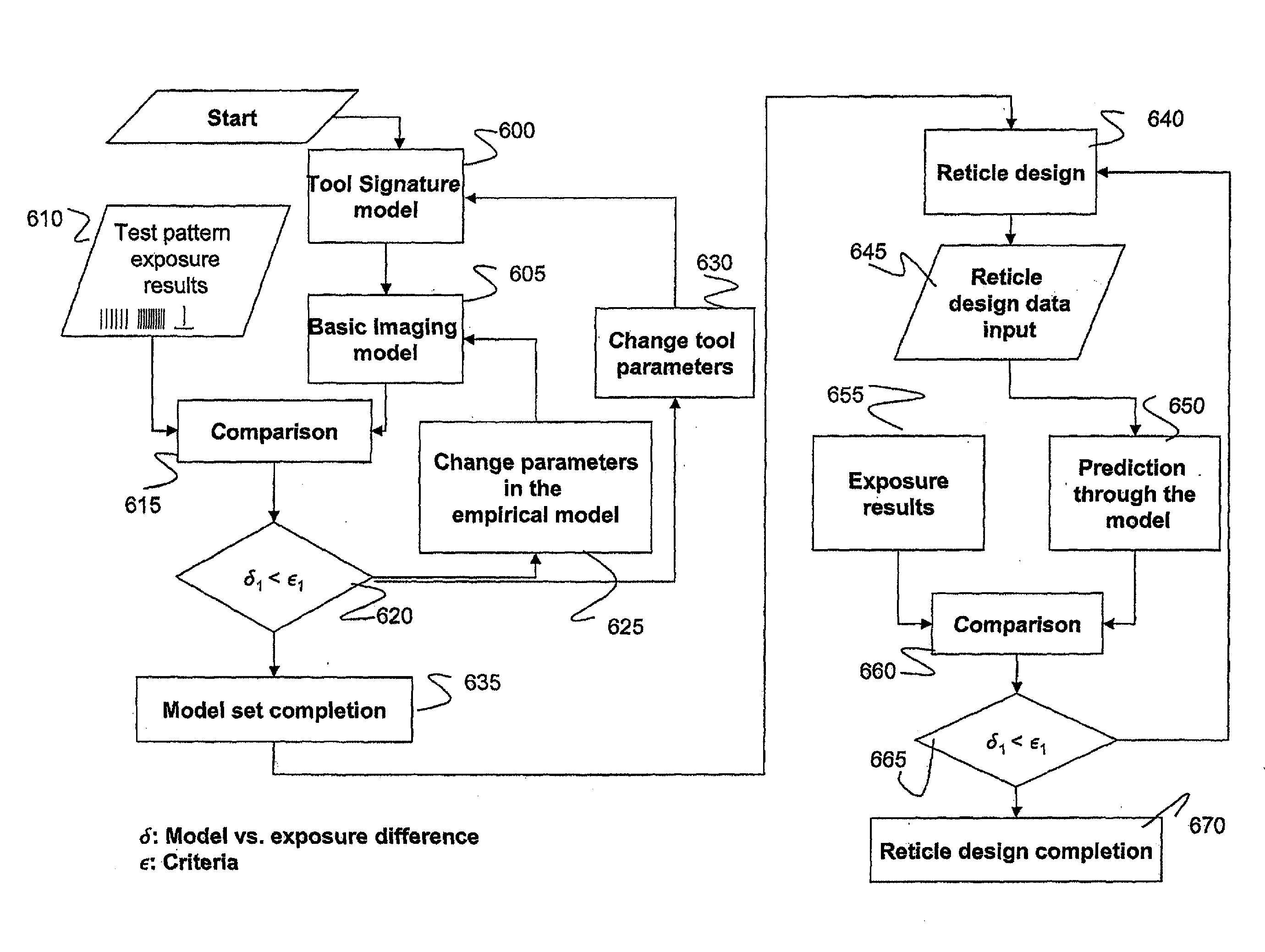
Scanner Based Optical Proximity Correction System and Method of Use
PatentActiveUS20100058263A1
Innovation
- A modeling technique that incorporates additional parameters such as illuminator details, lens signatures, flare data, chromatic aberrations, and synchronization errors into OPC models to generate a simulated, corrected reticle design, improving image fidelity and reducing the number of iterative cycles.

Semiconductor Manufacturing Standards and Regulations
The semiconductor manufacturing industry operates under a comprehensive framework of standards and regulations that directly impact computational lithography and optical proximity correction (OPC) implementation. International standards organizations such as SEMI (Semiconductor Equipment and Materials International) and IEEE establish critical guidelines for lithography processes, equipment specifications, and measurement protocols that govern how computational lithography techniques are developed and deployed across manufacturing facilities.
Regulatory compliance requirements vary significantly across global markets, with regions like the United States, European Union, and Asia-Pacific maintaining distinct approaches to semiconductor manufacturing oversight. The U.S. Department of Commerce's Bureau of Industry and Security (BIS) export administration regulations particularly influence the development and distribution of advanced computational lithography software and hardware systems. These regulations often restrict the transfer of cutting-edge OPC algorithms and computational lithography tools to certain countries, creating compliance challenges for multinational semiconductor companies.
Quality management standards, particularly ISO 9001 and automotive-specific IATF 16949, mandate rigorous documentation and validation procedures for computational lithography processes. These standards require manufacturers to maintain detailed records of OPC model development, calibration procedures, and process verification results. The implementation of statistical process control (SPC) methodologies becomes essential for monitoring the performance of computational lithography systems and ensuring consistent OPC effectiveness across production runs.
Environmental regulations significantly impact the selection and implementation of computational lithography solutions. The European Union's RoHS (Restriction of Hazardous Substances) directive and REACH (Registration, Evaluation, Authorization and Restriction of Chemicals) regulation influence the materials and chemicals used in photolithography processes that computational lithography techniques must accommodate. These environmental standards drive the development of more efficient OPC algorithms that can work effectively with environmentally compliant photoresist materials and processing chemicals.
Industry-specific standards such as JEDEC (Joint Electron Device Engineering Council) specifications define electrical and physical parameters that directly influence OPC strategy development. These standards establish critical dimension tolerances, overlay requirements, and defect density limits that computational lithography solutions must achieve. The continuous evolution of these standards, particularly for advanced node technologies, drives ongoing innovation in both computational lithography algorithms and OPC methodologies to meet increasingly stringent manufacturing requirements.
Cost-Performance Trade-offs in Lithography Enhancement
The economic considerations surrounding computational lithography and optical proximity correction represent a critical decision matrix for semiconductor manufacturers. Traditional OPC solutions typically require lower upfront capital investment, as they leverage established correction algorithms and can be implemented with existing computational infrastructure. However, as feature sizes continue to shrink below 7nm nodes, the computational complexity of OPC increases exponentially, leading to significant processing time penalties and higher operational costs per wafer.
Computational lithography approaches, while demanding substantial initial investments in advanced computing hardware and specialized software licenses, demonstrate superior cost-effectiveness at high-volume production scenarios. The parallel processing capabilities inherent in modern computational lithography systems enable faster turnaround times for complex mask designs, reducing the overall time-to-market for new semiconductor products. This acceleration becomes particularly valuable when considering the revenue implications of delayed product launches in competitive markets.
Performance metrics reveal distinct trade-off patterns between these technologies. OPC excels in scenarios requiring moderate correction complexity, delivering acceptable results with predictable computational overhead. The technology demonstrates linear scaling characteristics, making cost projections relatively straightforward for manufacturing planning purposes. However, performance degradation becomes pronounced when addressing advanced node requirements, where proximity effects become increasingly non-linear and difficult to model accurately.
Advanced computational lithography techniques, including machine learning-enhanced correction algorithms and full-chip simulation approaches, offer superior performance for cutting-edge applications but at significantly higher computational costs. These methods can achieve correction accuracies exceeding 95% for critical dimensions, compared to 85-90% typical for conventional OPC approaches. The performance advantage becomes more pronounced as design complexity increases, particularly for logic devices with dense, irregular patterns.
The cost-performance optimization point varies significantly based on production volume, node requirements, and design complexity. High-volume manufacturers processing advanced nodes typically find computational lithography approaches cost-justified within 12-18 months, while smaller fabs or those focused on mature nodes may find traditional OPC solutions more economically viable for extended periods.
Unlock deeper insights with Patsnap Eureka Quick Research — get a full tech report to explore trends and direct your research. Try now!
Generate Your Research Report Instantly with AI Agent
Supercharge your innovation with Patsnap Eureka AI Agent Platform!