

Evaluating Self-Assembled Monolayers in Smart Material Applications
SEP 29, 20259 MIN READ
Generate Your Research Report Instantly with AI Agent
PatSnap Eureka helps you evaluate technical feasibility & market potential.
SAM Technology Background and Objectives
Self-assembled monolayers (SAMs) represent a significant advancement in surface chemistry, emerging in the early 1980s through pioneering work by Nuzzo and Allara who demonstrated the spontaneous organization of alkanethiols on gold surfaces. This discovery marked the beginning of a revolutionary approach to molecular engineering at interfaces, enabling precise control over surface properties at the nanoscale. Over the past four decades, SAM technology has evolved from basic research into a versatile platform for modifying material surfaces across numerous applications.
The technological evolution of SAMs has been characterized by increasing sophistication in molecular design, deposition techniques, and characterization methods. Initially limited to simple thiol-gold systems, SAM technology now encompasses diverse molecular architectures on various substrates including silicon, metal oxides, and polymers. This expansion has been driven by advances in synthetic chemistry, allowing for the creation of functional SAMs with tailored properties such as specific wettability, biocompatibility, or sensing capabilities.
In the context of smart materials, SAMs serve as critical functional interfaces that can respond to external stimuli such as light, temperature, pH, or electrical signals. The integration of SAMs with smart materials has enabled the development of responsive surfaces that can dynamically alter their properties, facilitating applications in areas ranging from microfluidics to biomedical devices and advanced sensing platforms.
Current technological trends in SAM research focus on enhancing stability, functionality, and integration capabilities. Researchers are exploring mixed-monolayer systems, multi-component SAMs, and hierarchical surface structures to achieve more complex functionalities. Additionally, there is growing interest in developing SAMs that can undergo reversible conformational changes or chemical transformations in response to specific triggers, expanding their potential in dynamic smart material applications.
The primary objectives of SAM technology in smart material applications include achieving precise molecular control over surface properties, enhancing material responsiveness to environmental stimuli, improving durability under operational conditions, and enabling seamless integration with existing manufacturing processes. Researchers aim to develop SAMs that can serve as molecular switches, selective barriers, or transduction elements in smart material systems.
Looking forward, the field is moving toward multifunctional SAMs capable of simultaneous sensing and actuation, self-healing capabilities, and integration with emerging technologies such as flexible electronics and soft robotics. The ultimate goal is to harness the molecular precision of SAMs to create intelligent material interfaces that can adapt autonomously to changing conditions, opening new frontiers in materials science and engineering applications.
Market Analysis for SAM-Based Smart Materials
The global market for Self-Assembled Monolayer (SAM) based smart materials is experiencing significant growth, driven by increasing demand across multiple industries including electronics, healthcare, energy, and automotive sectors. Current market valuations indicate that the smart materials industry as a whole reached approximately 55 billion USD in 2022, with SAM-based technologies representing a rapidly expanding segment projected to grow at a compound annual growth rate of 12.3% through 2028.
Electronics and semiconductor industries currently dominate the application landscape for SAM-based smart materials, accounting for nearly 40% of market share. This dominance stems from the critical role SAMs play in miniaturization of electronic components, surface modification for improved conductivity, and development of next-generation sensing devices. The healthcare and biomedical sector follows closely, representing about 25% of the market, where SAMs are increasingly utilized in biosensors, drug delivery systems, and biocompatible coatings.
Regional analysis reveals North America and Europe as current market leaders, collectively holding approximately 65% of the global market share. However, the Asia-Pacific region, particularly China, South Korea, and Japan, demonstrates the fastest growth trajectory with increasing investments in research and manufacturing capabilities for advanced materials. This regional shift is expected to significantly alter market dynamics over the next five years.
Consumer demand trends indicate growing preference for multifunctional smart materials that can respond to multiple stimuli simultaneously. SAM-based materials that can self-heal, change properties based on environmental conditions, or integrate seamlessly with IoT systems are witnessing particularly strong market traction. This trend aligns with broader industry movements toward sustainable, energy-efficient, and adaptable material solutions.
Key market drivers include increasing miniaturization requirements in electronics, growing demand for advanced medical devices, expanding renewable energy infrastructure, and the push for more efficient automotive components. Regulatory environments are generally favorable, with governments worldwide implementing policies to support advanced materials research and commercialization.
Market challenges primarily revolve around scalability issues, with current SAM production methods facing limitations in large-scale manufacturing environments. Cost factors also present barriers to wider adoption, particularly in price-sensitive application areas. Additionally, knowledge gaps regarding long-term stability and performance of SAM-based smart materials in real-world conditions create market hesitation among potential industrial adopters.
Forecasts suggest that as manufacturing processes mature and economies of scale are achieved, SAM-based smart materials will experience accelerated market penetration, potentially disrupting traditional material supply chains across multiple industries within the next decade.
Current SAM Development Status and Challenges
Self-assembled monolayers (SAMs) have emerged as a significant area of research in materials science, with applications spanning from biosensors to electronic devices. Currently, the global development of SAM technology demonstrates varying levels of maturity across different application domains. In academic research, SAMs have been extensively studied for their fundamental properties and potential applications, with thousands of publications annually exploring novel chemistries and assembly techniques.
The industrial implementation of SAM technology, however, remains at a relatively early stage compared to its theoretical development. While certain sectors such as microelectronics and medical diagnostics have begun incorporating SAMs into commercial products, widespread adoption faces several critical challenges. These include scalability issues when transitioning from laboratory-scale production to industrial manufacturing, as well as concerns regarding the long-term stability of these molecular structures under real-world operating conditions.
Technical challenges in SAM development primarily revolve around three key areas: molecular design optimization, assembly process control, and performance consistency. The molecular architecture of SAMs must be precisely engineered to achieve desired surface properties, which requires sophisticated synthesis techniques and extensive characterization. Current methodologies often struggle to produce SAMs with uniform coverage and predictable orientation across large surface areas.
Process control represents another significant hurdle, as environmental factors such as temperature, humidity, and substrate cleanliness dramatically impact SAM formation. Even minor variations in these parameters can lead to defects in the monolayer structure, compromising functionality. The development of robust, reproducible assembly protocols remains an active area of research, with particular emphasis on techniques compatible with existing manufacturing infrastructure.
Geographically, SAM research and development exhibits distinct regional characteristics. North American institutions lead in fundamental research and patent generation, while Asian manufacturers, particularly in Japan and South Korea, have made significant advances in scaling production techniques. European research centers have focused on specialized applications, especially in biomedical interfaces and environmental sensing technologies.
Recent technological breakthroughs have partially addressed some of these challenges, including the development of vapor-phase deposition methods that improve uniformity, and the introduction of multi-component SAMs that enhance stability. However, the integration of SAMs with other emerging technologies, such as flexible electronics and responsive materials, introduces additional complexities that require interdisciplinary approaches to overcome.
The standardization of characterization methods and performance metrics represents another ongoing challenge, as the lack of universally accepted testing protocols hampers comparative analysis and technology transfer between research institutions and industry partners.
Current SAM Implementation Solutions
01 Fabrication and preparation methods of SAMs
Various techniques for creating self-assembled monolayers on different substrates, including solution-based deposition, vapor deposition, and microcontact printing. These methods control the formation of organized molecular structures with specific functional groups on surfaces. The preparation conditions such as concentration, temperature, and immersion time significantly affect the quality and properties of the resulting SAMs.- Fabrication methods for SAMs: Various techniques are employed to create Self-Assembled Monolayers on different substrates. These methods include vapor deposition, solution-based assembly, and microcontact printing. The fabrication process typically involves the spontaneous organization of molecules on surfaces through chemisorption, resulting in well-ordered molecular structures. These techniques allow for precise control over surface properties and can be optimized for different substrate materials and molecular components.
- Applications in biosensing and biomedical devices: Self-Assembled Monolayers serve as crucial interfaces in biosensing platforms and biomedical devices. They provide functional surfaces for the immobilization of biomolecules such as proteins, DNA, and antibodies. SAMs enable controlled interactions between biological components and device surfaces, improving sensitivity and specificity in diagnostic applications. The ability to tailor surface chemistry through SAMs allows for the development of biocompatible coatings, drug delivery systems, and implantable medical devices with enhanced performance and reduced biofouling.
- Electronic and optoelectronic applications: Self-Assembled Monolayers play a significant role in electronic and optoelectronic devices by modifying interfacial properties. They can be used to control charge transport, tune work functions, and improve device performance in organic electronics, field-effect transistors, and photovoltaic cells. SAMs provide nanoscale insulating or conducting layers that enable the fabrication of molecular electronic components. Additionally, they can modify optical properties of surfaces for applications in displays, sensors, and photonic devices.
- Surface modification and functionalization: Self-Assembled Monolayers offer versatile approaches for surface modification and functionalization across various materials. By selecting appropriate molecular components with specific terminal groups, surfaces can be engineered to exhibit desired properties such as hydrophobicity, hydrophilicity, or specific chemical reactivity. This enables the creation of surfaces with anti-fouling properties, controlled adhesion, corrosion resistance, or specific binding capabilities. The ability to pattern SAMs at micro and nanoscales allows for the development of complex surface architectures with spatially controlled functionality.
- Novel SAM materials and compositions: Research on Self-Assembled Monolayers has expanded to include novel molecular building blocks and compositions that enhance functionality and stability. These include thiol-based SAMs on gold, silane-based SAMs on oxide surfaces, phosphonic acid SAMs on metal oxides, and various hybrid systems. Recent developments focus on stimuli-responsive SAMs that can change properties in response to external triggers such as light, temperature, or electrical potential. Mixed-component SAMs combining different molecular species enable multifunctional surfaces with tunable properties for advanced applications.
02 Surface modification and functionalization using SAMs
Self-assembled monolayers are used to modify surface properties of various materials by introducing specific functional groups. This enables control over wettability, adhesion, friction, and biocompatibility. The functionalized surfaces can be tailored for specific applications by selecting appropriate terminal groups in the SAM molecules, creating surfaces with desired chemical, physical, and biological properties.Expand Specific Solutions03 SAMs in biosensing and biomedical applications
Self-assembled monolayers serve as platforms for biosensing and biomedical applications by providing controlled interfaces between biological systems and artificial materials. They can immobilize biomolecules such as proteins, DNA, and cells while maintaining their biological activity. These functionalized surfaces enable the development of biosensors, biocompatible implants, drug delivery systems, and diagnostic platforms with enhanced sensitivity and specificity.Expand Specific Solutions04 SAMs in electronic and optoelectronic devices
Self-assembled monolayers are utilized in electronic and optoelectronic devices to control charge transport, modify work functions, and create functional interfaces. They can serve as dielectric layers, electron transport layers, or hole transport layers in organic electronics. SAMs also enable the fabrication of molecular electronic devices, organic field-effect transistors, and improve the performance of solar cells and light-emitting devices.Expand Specific Solutions05 Patterning and lithography using SAMs
Self-assembled monolayers are employed in micro and nanofabrication processes as resist materials or templates for patterning. They can be selectively patterned using techniques such as photolithography, electron beam lithography, or microcontact printing. These patterned SAMs direct the deposition or etching of materials, enabling the fabrication of complex micro and nanostructures for applications in electronics, photonics, and microfluidics.Expand Specific Solutions
Key Industry Players in SAM Research
The self-assembled monolayers (SAMs) market in smart materials is currently in a growth phase, with increasing applications across electronics, sensors, and biomedical devices. The competitive landscape features established semiconductor companies like TSMC, Samsung Electronics, and NXP Semiconductors focusing on integration with existing manufacturing processes, while research institutions including MIT, Harvard, and University of California drive fundamental innovations. IBM and Infineon Technologies are leveraging SAMs for next-generation computing applications, while specialized companies like Surmodics and 3M Innovative Properties develop surface modification technologies for specific industry applications. The technology is approaching commercial maturity in certain segments, though broader implementation across diverse smart material applications requires further development of scalable manufacturing processes and standardization.
Battelle Memorial Institute
Technical Solution: Battelle has developed robust SAM-based smart material technologies focused on industrial applications and durability. Their approach centers on creating highly stable SAMs that maintain functionality in harsh environments, including extreme temperatures, chemical exposure, and mechanical stress. Battelle's platform utilizes phosphonic acid-based SAMs that form exceptionally strong bonds with metal oxide surfaces, providing superior stability compared to traditional thiol or silane systems. Their technology includes SAMs with embedded sensing capabilities that can detect structural changes, corrosion, or contamination in real-time, enabling predictive maintenance in industrial settings. Battelle researchers have also developed multi-component SAMs that combine protective and functional properties, such as corrosion resistance with electrical conductivity or antimicrobial activity. A key innovation is their work on scalable deposition methods for SAMs, including vapor-phase techniques that enable uniform coating of complex geometries and large surface areas for commercial applications.
Strengths: Exceptional durability in harsh industrial environments; excellent scalability for commercial applications; strong focus on practical implementation and cost-effectiveness. Weaknesses: Sometimes sacrifices molecular precision for robustness; more limited responsiveness compared to academic research systems; fewer options for biomedical applications due to focus on industrial durability.
President & Fellows of Harvard College
Technical Solution: Harvard has developed a comprehensive platform for self-assembled monolayers (SAMs) in smart materials focusing on dynamic, reconfigurable interfaces. Their approach utilizes electrochemically-controlled SAMs that can switch between hydrophilic and hydrophobic states in response to applied voltage, enabling smart surfaces for microfluidic applications. Harvard researchers have pioneered photo-switchable SAMs incorporating azobenzene derivatives that undergo conformational changes when exposed to specific wavelengths of light, creating surfaces with programmable adhesion properties. Their technology also includes SAMs with integrated molecular recognition elements that can selectively bind target molecules and trigger cascading responses in the material. A significant innovation is their work on SAM gradients—surfaces with continuously varying compositions that enable directional movement of liquids and particles without external energy input. Harvard has also developed SAMs with self-healing capabilities that can restore their functional properties after damage through dynamic molecular rearrangement processes.
Strengths: Highly sophisticated molecular design enabling precise control over surface properties; excellent integration of multiple stimuli-responsive mechanisms; innovative approaches to self-healing materials. Weaknesses: Complex synthesis procedures for specialized SAM molecules; some systems require controlled environments to maintain functionality; challenges in scaling up production for industrial applications.
Critical SAM Technical Innovations
Backfilled, self-assembled monolayers and methods of making same
PatentInactiveUS7553547B2
Innovation
- The use of a backfilling organosilane species, sequentially deposited with a relaxation agent, to enhance the chemical activity and stability of the monolayer by minimizing ligand-ligand and ligand-substrate interactions, allowing for improved analyte binding and monolayer density.


Molecular design to suppress desorption of self-assembled monolayers
PatentInactiveUS11002730B2
Innovation
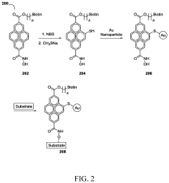
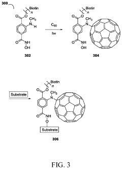
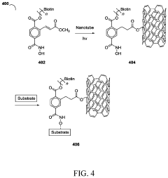
- Incorporating a mass altering unit, such as polymers, fullerenes, or nanoparticles, into the self-assembled monolayer on metal, metal oxide, or silicon-containing substrates to increase the mass of the SAM, thereby reducing desorption without interfering with analyte binding, forming a molecular detector system.
Sustainability Impact of SAM Technologies
The sustainability implications of Self-Assembled Monolayer (SAM) technologies extend far beyond their immediate technical applications, representing a significant paradigm shift in materials science with profound environmental consequences. When evaluating the ecological footprint of SAM technologies, their minimal material requirements stand out as a primary advantage. These molecular-scale coatings typically require only nanogram to microgram quantities of material per square centimeter of surface coverage, dramatically reducing resource consumption compared to traditional coating technologies that often demand orders of magnitude more material.
Energy efficiency represents another critical sustainability dimension of SAM applications. The self-assembly process occurs spontaneously at ambient or near-ambient conditions, eliminating the need for energy-intensive manufacturing processes such as high-temperature curing, vacuum deposition, or extensive solvent evaporation. This inherent energy efficiency translates to reduced carbon emissions throughout the production lifecycle, aligning with global decarbonization initiatives.
From a waste management perspective, SAM technologies offer compelling advantages. Many SAM precursors can be synthesized from renewable feedstocks, including plant-derived thiols and silanes. Furthermore, the precision of molecular self-assembly minimizes chemical waste generation during application, with utilization rates frequently exceeding 90% compared to conventional coating methods that may waste 30-50% of input materials through overspray or excess application.
The longevity enhancement provided by SAM treatments contributes significantly to sustainability through extended product lifecycles. By protecting underlying materials from corrosion, fouling, and degradation, SAM coatings can extend the functional lifetime of components by 200-300% in certain applications. This extension directly reduces replacement frequency and associated manufacturing impacts, particularly valuable in resource-intensive industries like electronics and transportation.
Water conservation represents an often-overlooked sustainability benefit of SAM technologies. Hydrophobic SAM coatings can reduce water consumption in maintenance operations by creating easy-to-clean surfaces that require less frequent washing and minimal cleaning agents. In industrial applications, this translates to measurable reductions in process water requirements and wastewater generation.
Despite these advantages, several sustainability challenges remain unresolved. The environmental fate and potential toxicity of certain SAM precursors, particularly those containing fluorinated compounds, raise legitimate ecological concerns. Additionally, the specialized synthesis pathways for some SAM molecules involve hazardous reagents that require careful management to prevent environmental contamination. Future research must prioritize developing SAM systems based entirely on non-toxic, biodegradable precursors to fully realize their sustainability potential.
Intellectual Property Landscape for SAMs
The intellectual property landscape for Self-Assembled Monolayers (SAMs) has evolved significantly over the past three decades, reflecting the growing importance of this technology in smart material applications. Patent activity in this field began to accelerate in the early 1990s, with foundational patents focusing primarily on basic SAM formation techniques and simple applications in surface modification.
Key patent holders in the SAM domain include major chemical companies such as Dow Chemical, DuPont, and 3M, who have established substantial IP portfolios covering fundamental SAM chemistries and manufacturing processes. Academic institutions like MIT, Stanford University, and Harvard University have also secured significant patents, particularly in novel SAM applications and specialized functionalization techniques.
The geographical distribution of SAM-related patents reveals interesting patterns, with the United States historically dominating the landscape but facing increasing competition from China, Japan, and the European Union. Chinese patent filings in particular have shown exponential growth since 2010, especially in electronics and sensor applications of SAMs.
Patent classification analysis indicates several distinct technology clusters within the SAM intellectual property space. These include biosensing applications (approximately 28% of patents), electronic device interfaces (23%), corrosion protection (17%), medical device coatings (15%), and advanced manufacturing processes (12%), with the remaining patents covering miscellaneous applications.
Recent patent trends show increasing focus on stimuli-responsive SAMs that can change properties in response to external triggers, which is particularly relevant for smart material applications. There has also been a notable rise in patents combining SAMs with other advanced materials such as graphene, quantum dots, and metal-organic frameworks to create hybrid systems with enhanced functionality.
Freedom-to-operate considerations reveal several potential IP bottlenecks in the commercial development of SAM-based smart materials. Particularly challenging areas include specific thiol chemistries for gold surfaces, certain silane-based SAM formulations, and methods for creating gradient-property SAMs. Companies entering this space should conduct thorough IP due diligence to navigate these constraints.
The patent landscape also highlights emerging white space opportunities, particularly in the development of SAMs for flexible electronics, environmental remediation applications, and energy storage interfaces. These areas show relatively low patent density despite their significant commercial potential, suggesting opportunities for strategic IP development.
Unlock deeper insights with PatSnap Eureka Quick Research — get a full tech report to explore trends and direct your research. Try now!
Generate Your Research Report Instantly with AI Agent
Supercharge your innovation with PatSnap Eureka AI Agent Platform!