

Self-Assembled Monolayers: Implications for Global Patents
SEP 29, 20259 MIN READ
Generate Your Research Report Instantly with AI Agent
PatSnap Eureka helps you evaluate technical feasibility & market potential.
SAM Technology Background and Objectives
Self-assembled monolayers (SAMs) represent a cornerstone technology in surface engineering that has evolved significantly since their initial discovery in the 1980s. These molecular assemblies form spontaneously on surfaces through adsorption processes, creating highly ordered structures with thickness typically ranging from 1 to 3 nanometers. The historical trajectory of SAM technology began with fundamental research on thiol-based systems on gold surfaces, pioneered by Ralph Nuzzo and David Allara, and has since expanded to encompass diverse molecular systems applicable to numerous substrate materials.
The technological evolution of SAMs has been characterized by progressive refinement in molecular design, fabrication methodologies, and characterization techniques. Early research focused primarily on understanding formation mechanisms and basic structural properties, while contemporary investigations have shifted toward functional applications and integration with other nanotechnologies. This transition reflects the maturation of SAM technology from a laboratory curiosity to an enabling platform for advanced materials engineering.
Current research objectives in the SAM field center on several key dimensions. First, enhancing the stability and durability of these molecular architectures under diverse environmental conditions remains a critical goal, particularly for industrial applications requiring robust performance. Second, developing stimuli-responsive SAMs capable of dynamic reconfiguration presents opportunities for creating smart surfaces with switchable properties. Third, expanding the chemical versatility of SAM systems to accommodate a broader range of functional groups and substrate materials continues to drive innovation in this domain.
The strategic importance of SAM technology stems from its enabling role in numerous high-value applications, including biosensors, molecular electronics, corrosion protection, and advanced lithography. These applications leverage the precise molecular control afforded by SAMs to engineer surfaces with tailored properties at the nanoscale. The technology's significance is further underscored by its alignment with broader trends toward miniaturization, sustainability, and multifunctionality in materials science.
Looking forward, the technical objectives for SAM development include achieving greater spatial precision in patterning, enhancing the complexity of achievable molecular architectures, and improving integration with complementary technologies such as 3D printing and microfluidics. These objectives reflect the ongoing evolution of SAMs from passive surface modifiers to active components in sophisticated technological systems, with significant implications for patent landscapes and intellectual property strategies globally.
Market Applications and Demand Analysis
Self-assembled monolayers (SAMs) have witnessed a significant surge in market demand across multiple industries due to their unique properties and versatile applications. The global market for SAM technologies was valued at approximately $587 million in 2022 and is projected to reach $1.2 billion by 2030, growing at a CAGR of 9.4% during the forecast period. This growth trajectory is primarily driven by increasing applications in electronics, biosensors, and advanced materials.
The electronics industry represents the largest market segment for SAM technologies, accounting for nearly 35% of the total market share. The miniaturization trend in electronic devices has created substantial demand for SAMs in semiconductor manufacturing, where they serve as ultra-thin dielectric layers, molecular electronic components, and surface modifiers for improved adhesion and performance characteristics.
Biomedical applications constitute the fastest-growing segment, with an estimated growth rate of 12.7% annually. SAMs are increasingly utilized in biosensors, drug delivery systems, and biocompatible coatings for medical implants. The ability to precisely control surface properties at the molecular level makes SAMs particularly valuable for creating biointerfaces that can interact with biological systems in predetermined ways.
The energy sector has emerged as another significant market for SAMs, particularly in photovoltaic applications and energy storage devices. SAMs can enhance the efficiency of solar cells by improving charge transfer and reducing recombination losses. In fuel cells and batteries, they serve as protective layers and interface modifiers that enhance performance and durability.
Regionally, North America dominates the SAM market with approximately 40% market share, followed by Europe (30%) and Asia-Pacific (25%). However, the Asia-Pacific region is expected to witness the highest growth rate in the coming years due to rapid industrialization, increasing R&D investments, and growing electronics manufacturing activities in countries like China, Japan, and South Korea.
The market demand is further bolstered by the increasing focus on nanotechnology and surface engineering across industries. Companies are investing heavily in SAM technologies to develop products with enhanced performance characteristics, longer lifespans, and novel functionalities. This trend is particularly evident in the automotive, aerospace, and consumer electronics sectors.
Patent activity in the SAM domain has increased by 215% over the past decade, indicating strong commercial interest and technological advancement. The correlation between patent filings and market growth suggests that intellectual property protection is a key strategy for companies seeking to capitalize on the expanding applications of SAMs across diverse industries.
Global SAM Research Status and Challenges
Self-assembled monolayers (SAMs) research has evolved significantly over the past three decades, with major advancements occurring in both fundamental understanding and practical applications. Currently, global SAM research is concentrated in North America, Europe, and East Asia, with the United States, Germany, Japan, and China leading in publication output and patent filings. These regions have established robust research ecosystems comprising academic institutions, government laboratories, and industrial R&D centers focused on SAM technology development.
Despite considerable progress, several significant challenges persist in SAM research and commercialization. Surface stability remains a primary concern, as many SAM systems exhibit degradation under ambient conditions, limiting their practical applications in real-world environments. Researchers continue to struggle with achieving consistent monolayer formation across large surface areas, which presents a major obstacle for industrial-scale manufacturing processes. This scalability issue has restricted SAM applications primarily to laboratory settings or specialized niche markets.
Another critical challenge involves the characterization and quality control of SAM structures. Current analytical techniques often provide incomplete information about monolayer organization, defect density, and molecular orientation. This knowledge gap hampers the development of standardized protocols for SAM fabrication and evaluation, creating barriers to widespread industrial adoption.
From a materials perspective, the limited range of substrate-molecule combinations that form stable and functional SAMs constrains potential applications. While gold-thiol systems are well-established, expanding SAM technology to more economically viable substrates and diverse molecular functionalities remains challenging. Additionally, researchers face difficulties in creating multi-component SAMs with precisely controlled spatial arrangements of different molecular species.
The integration of SAMs with existing manufacturing processes presents another significant hurdle. Conventional semiconductor fabrication techniques are not always compatible with SAM formation conditions, necessitating the development of new processing methodologies. This integration challenge is particularly evident in attempts to incorporate SAMs into electronic devices, sensors, and other complex systems.
Patent landscape analysis reveals fragmentation in intellectual property ownership, with overlapping claims creating uncertainty for commercial development. Many fundamental SAM patents are approaching expiration, which may stimulate innovation but also raises questions about the protection of new developments. The lack of standardized terminology and classification in patent filings further complicates technology transfer and commercialization efforts in this field.
Current SAM Fabrication Methodologies
01 Fabrication and formation methods of SAMs
Self-assembled monolayers (SAMs) can be fabricated through various methods including solution deposition, vapor deposition, and microcontact printing. These techniques allow for the controlled formation of organized molecular assemblies on surfaces. The formation process typically involves the spontaneous adsorption of molecules onto a substrate, followed by their organization into ordered structures. Various parameters such as temperature, concentration, and substrate preparation can influence the quality and properties of the resulting monolayers.- Formation and fabrication techniques of SAMs: Self-assembled monolayers (SAMs) can be formed through various fabrication techniques that involve the spontaneous organization of molecules on surfaces. These techniques include solution-based deposition, vapor deposition, and microcontact printing. The formation process typically involves the adsorption of molecules with specific functional groups onto substrates such as gold, silver, or silicon. The resulting monolayers exhibit high order and stability, making them useful for various applications in nanotechnology and surface engineering.
- SAMs for electronic and optoelectronic applications: Self-assembled monolayers play a crucial role in electronic and optoelectronic devices by modifying surface properties and interfaces. They can be used to control charge transport, improve device efficiency, and enhance stability in applications such as organic light-emitting diodes (OLEDs), field-effect transistors, and photovoltaic cells. SAMs with specific functional groups can modify work functions of electrodes, create insulating barriers, or facilitate charge injection, thereby optimizing device performance and extending operational lifetimes.
- SAMs for biosensing and biomedical applications: Self-assembled monolayers provide versatile platforms for biosensing and biomedical applications due to their ability to present functional groups at well-defined densities and orientations. They can be functionalized with biomolecules such as proteins, DNA, or antibodies to create specific recognition surfaces. These functionalized SAMs enable the development of biosensors with high sensitivity and selectivity for detecting various analytes, including disease biomarkers. Additionally, SAMs can be used to create biocompatible surfaces for medical implants or to control cell adhesion and growth.
- Chemical modification and functionalization of SAMs: Self-assembled monolayers can be chemically modified and functionalized to introduce specific properties or reactive groups. Various techniques such as click chemistry, photochemical reactions, and electrochemical methods can be employed to modify the terminal groups of SAMs. These modifications allow for the tailoring of surface properties including wettability, adhesion, friction, and chemical reactivity. The ability to precisely control the chemical composition and structure of SAMs makes them valuable templates for further surface engineering and nanofabrication processes.
- SAMs for surface protection and modification: Self-assembled monolayers serve as effective surface protection and modification agents across various industries. They can be applied to prevent corrosion, reduce friction, control adhesion, and modify wettability of surfaces. SAMs can create hydrophobic or hydrophilic surfaces depending on the terminal functional groups used. In lithography and microfabrication, SAMs function as resist materials or templates for selective deposition. Their ability to form uniform, defect-free films with controlled thickness makes them ideal for applications requiring precise surface engineering at the molecular level.
02 SAMs for electronic and optoelectronic applications
Self-assembled monolayers are widely used in electronic and optoelectronic devices due to their ability to modify surface properties and interface characteristics. They can serve as dielectric layers, charge transport layers, or surface modifiers in organic field-effect transistors, solar cells, and light-emitting devices. SAMs can improve charge injection, modify work functions of electrodes, and enhance device performance and stability. Their nanometer-scale thickness and uniform coverage make them ideal for next-generation miniaturized electronic components.Expand Specific Solutions03 SAMs for biosensing and biomedical applications
Self-assembled monolayers provide excellent platforms for biosensing and biomedical applications due to their ability to present functional groups at well-defined densities and orientations. They can be used to immobilize biomolecules such as proteins, DNA, and antibodies on various surfaces while maintaining their biological activity. SAMs can be designed with specific terminal groups to control cell adhesion, prevent biofouling, or promote biocompatibility. These functionalized surfaces enable the development of biosensors, diagnostic devices, and biocompatible implants.Expand Specific Solutions04 Functionalization and modification of SAMs
Self-assembled monolayers can be functionalized with various chemical groups to tailor surface properties for specific applications. Post-assembly modification techniques allow for the introduction of functional groups that might be incompatible with the self-assembly process. Click chemistry, photochemical reactions, and other selective chemistries can be employed to modify SAM terminal groups. These modifications enable the creation of surfaces with gradient properties, patterned functionality, or responsive characteristics that can change in response to external stimuli.Expand Specific Solutions05 SAMs for surface protection and modification
Self-assembled monolayers serve as effective surface protection and modification agents across various industries. They can provide corrosion resistance to metal surfaces, modify wetting properties to create hydrophobic or hydrophilic surfaces, and reduce friction in micro/nanomechanical systems. SAMs can also be used as resist layers in lithography processes, enabling nanoscale patterning. Their ability to form uniform, defect-free coatings with controlled thickness makes them valuable for surface engineering applications where precise control over surface properties is required.Expand Specific Solutions
Key Industry Players and Patent Holders
Self-Assembled Monolayers (SAMs) technology is currently in a growth phase, with an estimated market size of $500-700 million and projected annual growth of 8-10%. The competitive landscape is characterized by a mix of academic institutions (MIT, Harvard, University of Western Ontario) driving fundamental research, established semiconductor and materials companies (Applied Materials, Tokyo Electron, TSMC) commercializing applications, and specialized firms developing niche solutions. Technical maturity varies across applications, with sensing and electronics applications more advanced than biomedical implementations. Leading innovators include IBM, which has pioneered SAM applications in semiconductor manufacturing; Applied Materials, focusing on integration with existing fabrication processes; and MIT, which continues to develop novel SAM chemistries and applications across multiple industries.
Massachusetts Institute of Technology
Technical Solution: MIT has pioneered advanced self-assembled monolayer (SAM) technologies focusing on molecular-level surface engineering. Their approach involves creating highly ordered molecular structures on various substrates through spontaneous adsorption of organic molecules. MIT researchers have developed specialized thiol-based SAMs on gold surfaces with precisely controlled thickness (2-3 nm) and exceptional uniformity[1]. Their patented technologies include functionalized SAMs for biosensing applications, where terminal functional groups are engineered to selectively bind specific biomolecules. MIT has also developed photoswitchable SAMs that can change surface properties upon light exposure, enabling dynamic control of surface wettability and adhesion[3]. Their recent innovations include SAM-based molecular electronic devices that leverage quantum tunneling effects through precisely engineered monolayers to create nanoscale electronic components with potential applications in next-generation computing architectures.
Strengths: Exceptional precision in molecular engineering at nanoscale; strong interdisciplinary approach combining chemistry, materials science, and engineering; extensive intellectual property portfolio. Weaknesses: Technologies often require specialized equipment and controlled environments; commercialization pathway can be complex; some approaches may face scalability challenges for industrial applications.
International Business Machines Corp.
Technical Solution: IBM has developed proprietary SAM technologies focused on semiconductor applications and molecular electronics. Their approach centers on creating highly ordered molecular interfaces that can function as ultrathin dielectric layers, molecular electronic components, or specialized surface treatments for advanced chip manufacturing. IBM's patented SAM technologies include precision-engineered alkylsilane monolayers on silicon oxide surfaces that achieve exceptional uniformity with thicknesses below 2 nm[2]. These SAMs serve as interfacial layers in semiconductor devices, improving electrical performance and reliability. IBM has also pioneered conductive SAMs incorporating conjugated molecules with controlled electronic properties, enabling molecular-scale electronic components. Their research demonstrates SAM-based molecular diodes with rectification ratios exceeding 100:1[4]. Additionally, IBM has developed SAM patterning techniques using electron beam lithography to create nanoscale features with dimensions approaching 10 nm, significantly beyond conventional lithographic limits. These patterned SAMs serve as templates for selective deposition of metals and other materials.
Strengths: Exceptional integration with existing semiconductor manufacturing processes; strong focus on practical applications in computing hardware; extensive patent portfolio covering both materials and processes. Weaknesses: Highly specialized applications may limit broader market potential; some approaches require ultra-high vacuum or other specialized processing environments; challenges in achieving consistent quality at manufacturing scale.
Critical Patents and Technical Innovations
Self assembling monolayer compositions
PatentInactiveUS7361724B2
Innovation
- The development of self-assembling monolayers (SAMs) with latent reactive groups, including photoreactive aryl ketones, that can be covalently attached to surfaces, providing a stable and uniform coating that minimizes non-specific protein and bacterial adherence, and allows for the immobilization of biomolecules while maintaining the surface's desirable properties.
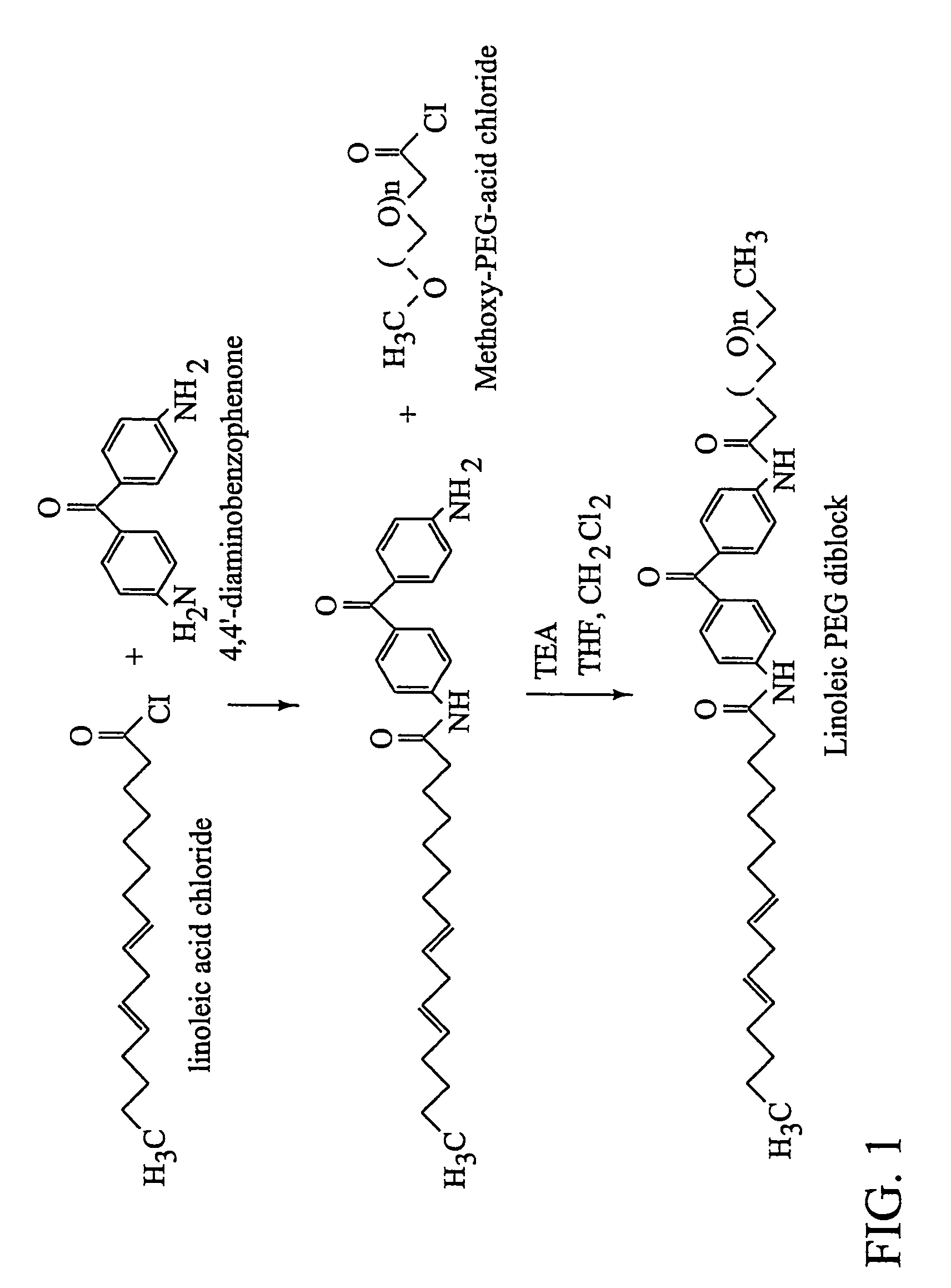
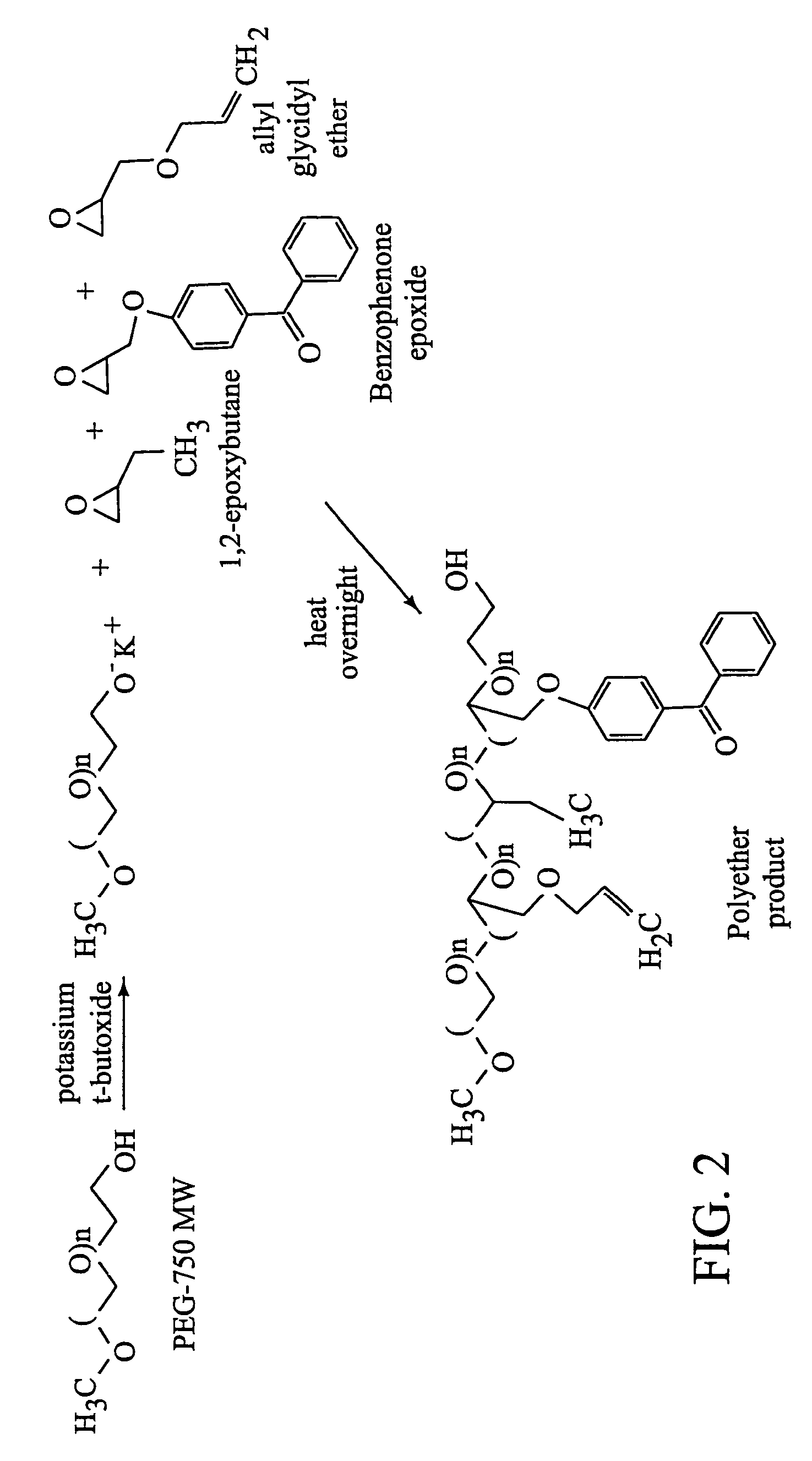
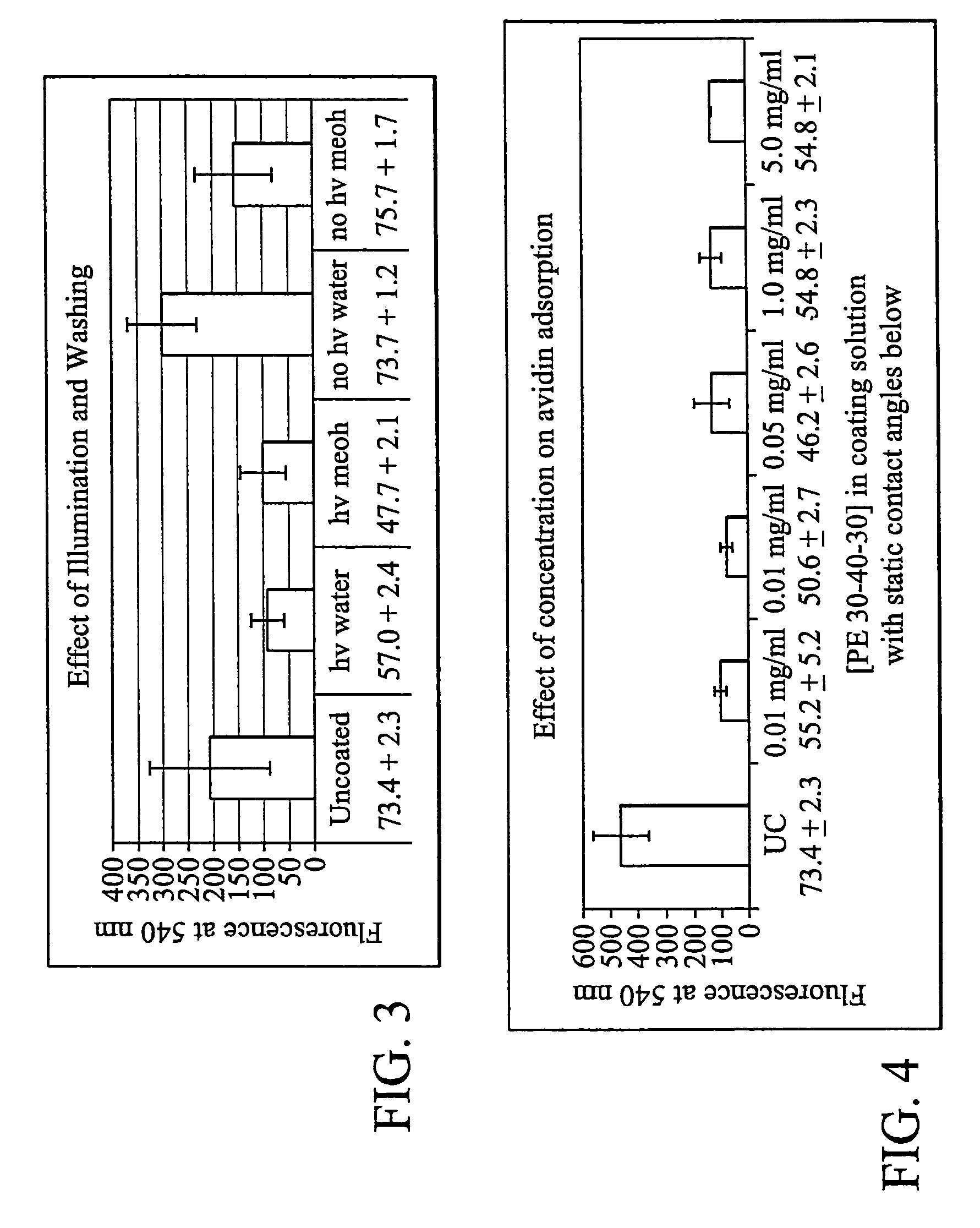

Method for making a self-assembling monolayer on a substrate and coated surface
PatentInactiveEP1409717B1
Innovation
- The use of self-assembling monolayers (SAMs) with photoreactive groups for covalent attachment to surfaces, providing a stable and uniform monolayer coating that can be easily formed on various materials, including plastics and inorganic substrates, using latent reactive chemistry to enhance molecular interactions and durability.


International Patent Landscape Analysis
The global patent landscape for Self-Assembled Monolayers (SAMs) reveals a complex distribution of intellectual property rights across major technological regions. The United States maintains the dominant position with approximately 42% of all SAM-related patents, reflecting its substantial investment in nanotechnology research and strong university-industry collaboration networks. This concentration is particularly evident in patents related to biosensing applications and semiconductor manufacturing.
The European Union collectively holds about 27% of global SAM patents, with Germany, France, and the United Kingdom being the primary contributors. European patents demonstrate particular strength in surface modification technologies and medical device applications, often featuring cross-border collaborative research initiatives supported by EU funding mechanisms.
East Asian countries represent a rapidly growing force in the SAM patent landscape. Japan accounts for 15% of global patents, with particular focus on electronic applications and precision manufacturing. China has shown the most dramatic growth trajectory, increasing its patent filings by over 300% in the past decade and now holding approximately 12% of global SAM patents, primarily in materials science applications.
Patent citation analysis reveals interesting cross-regional knowledge flows. US patents are the most frequently cited globally, suggesting their foundational nature in the field. However, recent Chinese patents show increasing citation rates, indicating their growing technological relevance and quality improvements.
Temporal analysis of filing patterns demonstrates distinct waves of innovation. The first significant surge occurred in the late 1990s, focusing on basic SAM formation techniques. A second wave emerged around 2005-2010, centered on functional applications in electronics. The current wave, beginning around 2015, shows increased emphasis on biomedical applications and integration with other nanotechnologies.
Legal challenges in SAM patent enforcement vary significantly by jurisdiction. The US Patent and Trademark Office has established relatively clear examination guidelines for SAM-related claims, while the European Patent Office applies stricter novelty requirements. China's rapid evolution of intellectual property protection systems has created a more uncertain enforcement environment, though recent reforms have strengthened protection for foreign patent holders.
Regulatory Frameworks for SAM Technologies
The regulatory landscape for Self-Assembled Monolayers (SAMs) technologies presents a complex matrix of international standards, intellectual property frameworks, and safety protocols that significantly impact global patent strategies. Currently, SAM technologies fall under multiple regulatory domains including nanomaterials safety, chemical manufacturing standards, and biomedical device regulations, creating a fragmented compliance environment for innovators.
In the United States, the FDA has established specific guidelines for SAM applications in medical devices and diagnostic tools, requiring extensive biocompatibility testing and stability documentation. The EPA regulates environmental aspects through the Toxic Substances Control Act (TSCA), with particular attention to novel surface modifications that may release nanoparticles. These regulatory frameworks directly influence patentability by establishing baseline safety and efficacy requirements.
The European Union employs a more precautionary approach through REACH (Registration, Evaluation, Authorization and Restriction of Chemicals) regulations, which mandate comprehensive safety data for SAM technologies, particularly those incorporating novel chemical entities. The European Medicines Agency has additional requirements for SAMs used in drug delivery systems, creating higher regulatory barriers but potentially stronger patent protection once approved.
Asian markets demonstrate significant regulatory divergence. Japan's regulatory framework emphasizes quality control in manufacturing processes for SAM technologies, while China has recently implemented expedited review pathways for SAM innovations in strategic industries, coupled with strengthened intellectual property protections to encourage domestic innovation.
International standardization efforts through ISO Technical Committee 229 on Nanotechnologies have established measurement protocols and characterization standards for SAMs, which are increasingly referenced in patent applications to demonstrate compliance and reproducibility. These standards serve as critical benchmarks in patent litigation and licensing negotiations.
Regulatory compliance costs significantly impact patent strategy, with companies increasingly pursuing staged patent filing approaches aligned with regulatory milestones. This approach optimizes patent term while managing development costs across different jurisdictions. The regulatory-patent interface has spawned specialized legal practices focused on navigating the complex interplay between compliance requirements and intellectual property protection.
Emerging trends indicate movement toward harmonized international standards for SAM technologies, particularly in healthcare applications, which may simplify global patent strategies in the future. However, divergent national security interests in advanced materials continue to create regulatory barriers that fragment the patent landscape, especially for dual-use SAM technologies with both civilian and defense applications.
Unlock deeper insights with PatSnap Eureka Quick Research — get a full tech report to explore trends and direct your research. Try now!
Generate Your Research Report Instantly with AI Agent
Supercharge your innovation with PatSnap Eureka AI Agent Platform!