

Extreme Aspect Ratios in Computed Lithography: Solutions & Comparisons
APR 24, 20269 MIN READ
Generate Your Research Report Instantly with AI Agent
PatSnap Eureka helps you evaluate technical feasibility & market potential.
Extreme Aspect Ratio Lithography Background and Objectives
Extreme aspect ratio lithography has emerged as one of the most critical challenges in advanced semiconductor manufacturing, particularly as the industry pushes toward sub-3nm technology nodes. The evolution of lithographic processes has consistently demanded higher resolution capabilities, with aspect ratios now reaching unprecedented levels of 40:1 and beyond in deep trench structures, through-silicon vias, and advanced memory architectures.
The historical progression of lithography technology demonstrates a clear trajectory from simple planar structures to increasingly complex three-dimensional architectures. Early lithographic processes in the 1970s and 1980s dealt with relatively modest aspect ratios of 2:1 to 5:1. However, the relentless pursuit of Moore's Law scaling and the transition to 3D device architectures have fundamentally transformed the requirements, necessitating precise control over extremely narrow, deep features.
Contemporary semiconductor devices, particularly in NAND flash memory and DRAM applications, require vertical structures with aspect ratios exceeding 30:1. These structures present unique challenges in terms of photoresist coating uniformity, exposure dose distribution, and development process control. The physics of light propagation and chemical diffusion within such confined geometries creates complex interactions that traditional lithographic models struggle to predict accurately.
The primary technical objectives in extreme aspect ratio lithography center on achieving uniform critical dimension control throughout the entire depth of high-aspect-ratio features. This encompasses maintaining consistent linewidth, minimizing sidewall roughness, and ensuring complete pattern transfer without defects such as scumming, bridging, or incomplete development at the feature bottom.
Advanced computational lithography techniques have become indispensable tools for addressing these challenges. Optical proximity correction algorithms must now account for three-dimensional light scattering effects, while resist models require sophisticated treatment of diffusion-limited processes in confined geometries. The integration of machine learning approaches with traditional physical models represents a promising avenue for improving prediction accuracy and process robustness.
The ultimate goal extends beyond mere pattern fidelity to encompass manufacturing yield and economic viability. Successful extreme aspect ratio lithography solutions must demonstrate scalability across different device architectures while maintaining compatibility with existing fabrication infrastructure and meeting stringent cost-per-feature requirements that enable continued semiconductor industry growth.
Market Demand for High Aspect Ratio Semiconductor Structures
The semiconductor industry is experiencing unprecedented demand for high aspect ratio structures, driven by the relentless pursuit of device miniaturization and performance enhancement. Advanced memory technologies, particularly 3D NAND flash and DRAM, represent the primary market drivers for extreme aspect ratio lithography solutions. These memory architectures require vertical structures with aspect ratios exceeding 50:1, pushing the boundaries of conventional lithography capabilities.
The transition to advanced node technologies below 7nm has intensified the need for precise control over high aspect ratio features. Logic devices increasingly incorporate vertical transistor architectures, such as gate-all-around field-effect transistors and vertical nanowire structures, which demand exceptional dimensional control and uniformity across extreme aspect ratios. This architectural evolution directly correlates with the growing market demand for sophisticated computed lithography solutions.
Emerging applications in artificial intelligence and machine learning accelerators are creating new market segments requiring specialized high aspect ratio structures. These applications demand unique interconnect architectures and memory hierarchies that rely heavily on vertical integration strategies. The proliferation of edge computing devices and Internet of Things applications further amplifies the need for compact, high-performance semiconductor solutions with extreme aspect ratio features.
The automotive semiconductor market presents another significant growth driver, particularly with the advancement of autonomous driving technologies and electric vehicle systems. These applications require robust, high-density semiconductor solutions that often incorporate high aspect ratio structures for improved thermal management and electrical performance. Safety-critical automotive applications demand exceptional reliability and precision in manufacturing processes.
Market analysis indicates that foundries and memory manufacturers are investing heavily in advanced lithography equipment capable of handling extreme aspect ratio challenges. The economic pressure to maximize wafer utilization while achieving higher device densities creates a compelling business case for investing in computed lithography solutions that can reliably produce high aspect ratio structures.
The packaging industry also contributes to market demand through advanced packaging technologies such as through-silicon vias and high-density interconnects. These technologies require precise control over high aspect ratio features to enable heterogeneous integration and system-in-package solutions that meet the performance requirements of next-generation electronic systems.
Current Challenges in Extreme Aspect Ratio Lithography
Extreme aspect ratio lithography faces fundamental physical limitations that challenge conventional optical and computational approaches. The primary constraint stems from the wavelength-dependent diffraction limits, where features with aspect ratios exceeding 10:1 encounter severe optical proximity effects and pattern fidelity degradation. These limitations become particularly pronounced at advanced technology nodes below 7nm, where the gap between desired feature dimensions and available lithographic wavelengths continues to widen.
Pattern collapse represents a critical mechanical challenge in high aspect ratio structures. As feature heights increase relative to their width, capillary forces during wet processing steps can cause structural failure, leading to yield loss and pattern distortion. This phenomenon is exacerbated by the increasing use of low-k dielectric materials, which possess reduced mechanical strength compared to traditional silicon dioxide.
Computational lithography algorithms struggle with convergence issues when processing extreme aspect ratio patterns. Traditional optical proximity correction models, designed for moderate aspect ratios, exhibit numerical instability and extended computation times when applied to structures with ratios exceeding 8:1. The mathematical complexity increases exponentially as the aspect ratio grows, creating bottlenecks in mask optimization workflows.
Etch loading effects present another significant challenge, where high aspect ratio features experience non-uniform etch rates across the pattern field. This leads to critical dimension variations and profile distortions that cannot be adequately compensated through conventional bias adjustments. The interaction between plasma chemistry and narrow, deep trenches creates complex transport phenomena that are difficult to model accurately.
Metrology and inspection capabilities lag behind manufacturing requirements for extreme aspect ratio features. Current scanning electron microscopy techniques struggle to provide accurate three-dimensional measurements of deep, narrow structures, limiting process control feedback. This measurement gap creates uncertainty in process optimization and yield improvement efforts.
Resist material limitations further compound these challenges, as traditional photoresists lack the mechanical properties necessary to maintain structural integrity during development and subsequent processing steps. The trade-off between resolution, sensitivity, and line edge roughness becomes increasingly difficult to optimize for extreme geometries.
Existing Computational Solutions for Aspect Ratio Control
01 Computational lithography methods for optimizing mask patterns
Advanced computational lithography techniques are employed to optimize mask patterns by calculating and adjusting aspect ratios of features. These methods use optical proximity correction (OPC) and model-based algorithms to predict how patterns will transfer to wafers, accounting for diffraction effects and process variations. The computational approach enables precise control of feature dimensions and aspect ratios to achieve desired pattern fidelity on the substrate.- Computational lithography methods for optimizing mask patterns: Advanced computational lithography techniques are employed to optimize mask patterns by calculating and adjusting aspect ratios of features. These methods use optical proximity correction (OPC) and model-based algorithms to predict how patterns will transfer to wafers, accounting for diffraction effects and process variations. The computational approach allows for iterative refinement of mask designs to achieve desired feature geometries with optimal aspect ratios on the substrate.
- Aspect ratio control in photoresist feature formation: Methods for controlling the aspect ratio of photoresist features during lithographic patterning involve computational modeling of exposure and development processes. These techniques calculate optimal exposure doses, focus conditions, and resist thicknesses to achieve target aspect ratios. The computational models account for standing wave effects, resist contrast, and development kinetics to predict final feature profiles and their dimensional characteristics.
- Simulation-based verification of lithographic aspect ratios: Verification methodologies utilize computational simulation to validate that designed patterns will produce features with acceptable aspect ratios in manufacturing. These systems perform rigorous checks using lithography simulation engines that model the complete imaging process, including illumination, mask diffraction, and resist processing. The verification process identifies potential aspect ratio violations before mask fabrication, enabling design corrections.
- Resolution enhancement techniques for high aspect ratio features: Computational approaches for enabling high aspect ratio feature printing through resolution enhancement technologies. These methods include phase-shifting mask designs, off-axis illumination optimization, and sub-resolution assist feature placement, all calculated through sophisticated algorithms. The computational optimization balances multiple objectives including feature fidelity, process window, and manufacturability for structures with challenging aspect ratios.
- Machine learning and AI-based aspect ratio optimization: Modern computational lithography systems incorporate machine learning and artificial intelligence algorithms to optimize aspect ratios of lithographic features. These advanced methods learn from large datasets of simulation and experimental results to predict optimal process parameters and mask corrections. The AI-driven approaches can handle complex interactions between multiple variables affecting aspect ratio outcomes, providing faster and more accurate solutions than traditional computational methods.
02 Aspect ratio control in photoresist feature formation
Methods for controlling aspect ratios during photoresist patterning involve optimizing exposure conditions, resist thickness, and development parameters. The aspect ratio of photoresist features directly impacts pattern transfer quality and subsequent etching processes. Techniques include adjusting numerical aperture, illumination settings, and resist chemistry to achieve target aspect ratios while maintaining pattern integrity and minimizing defects.Expand Specific Solutions03 Resolution enhancement techniques for high aspect ratio features
Resolution enhancement technologies enable the creation of high aspect ratio features beyond conventional optical limits. These techniques include phase-shifting masks, off-axis illumination, and multiple patterning strategies. By manipulating the phase and intensity of light, these methods improve the depth of focus and allow for steeper sidewalls and higher aspect ratios in lithographic patterns, essential for advanced semiconductor nodes.Expand Specific Solutions04 Simulation and modeling of lithographic aspect ratios
Computational simulation tools are utilized to predict and analyze aspect ratios in lithographic processes before actual fabrication. These models incorporate optical, chemical, and physical parameters to simulate resist profile evolution and final feature geometry. Simulation enables optimization of process parameters and mask designs to achieve desired aspect ratios while identifying potential manufacturing issues early in the design cycle.Expand Specific Solutions05 Metrology and measurement of lithographic aspect ratios
Precise measurement techniques are essential for characterizing aspect ratios of lithographically defined features. Methods include scanning electron microscopy, atomic force microscopy, and optical scatterometry to determine feature height, width, and sidewall angles. Advanced metrology enables feedback control for process optimization and ensures that manufactured features meet specified aspect ratio requirements for device performance and reliability.Expand Specific Solutions
Key Players in Advanced Lithography Equipment Industry
The extreme aspect ratios in computed lithography field represents a mature but rapidly evolving segment within the semiconductor manufacturing industry, currently valued at approximately $15-20 billion globally. The industry is in an advanced development stage, driven by increasing demands for smaller node processes and complex 3D structures. Technology maturity varies significantly among key players, with established leaders like GLOBALFOUNDRIES, Tokyo Electron, and Synopsys demonstrating advanced computational lithography capabilities, while foundries such as SMIC and Shanghai Huali are rapidly developing competitive solutions. Research institutions including Imec, CEA, and Fudan University contribute cutting-edge innovations in extreme aspect ratio modeling and correction algorithms. Equipment manufacturers like Nikon, NuFlare Technology, and Tokyo Electron provide essential hardware platforms, while software leaders such as Siemens Industry Software and Synopsys offer sophisticated computational solutions for managing complex lithographic challenges in next-generation semiconductor manufacturing processes.
Siemens Industry Software, Inc.
Technical Solution: Siemens offers advanced computational lithography solutions through their Calibre platform, featuring specialized algorithms for extreme aspect ratio patterning challenges. Their approach combines physical modeling with machine learning techniques to optimize mask designs for high aspect ratio features. The Calibre nmOPC tool incorporates three-dimensional resist modeling that accurately predicts sidewall profiles and critical dimension variations in deep structures. Their solution includes advanced source mask optimization (SMO) capabilities that can simultaneously optimize illumination conditions and mask patterns for aspect ratios up to 15:1, demonstrating up to 35% improvement in process window compared to traditional OPC methods.
Strengths: Strong integration with manufacturing workflows, robust 3D modeling capabilities, excellent customer support. Weaknesses: Limited market share compared to competitors, higher learning curve for advanced features.
Nikon Corp.
Technical Solution: Nikon has developed specialized lithography systems and computational solutions to address extreme aspect ratio challenges in semiconductor manufacturing. Their approach focuses on advanced illumination optimization and pupil engineering techniques combined with computational lithography algorithms. The company's solution includes customized source shapes and polarization control that work in conjunction with inverse lithography technology to improve pattern transfer for high aspect ratio structures. Their computational framework incorporates rigorous coupled-wave analysis (RCWA) for accurate modeling of electromagnetic effects in deep features, enabling successful patterning of structures with aspect ratios exceeding 12:1 while maintaining critical dimension uniformity within ±3nm across the exposure field.
Strengths: Deep expertise in optical lithography systems, strong hardware-software integration, proven manufacturing solutions. Weaknesses: Limited software-only offerings, primarily focused on optical lithography rather than EUV applications.
Core Innovations in Extreme Aspect Ratio Processing
Method and apparatus for fracturing polygons on masks used in an optical lithography process
PatentInactiveUS6887630B2
Innovation
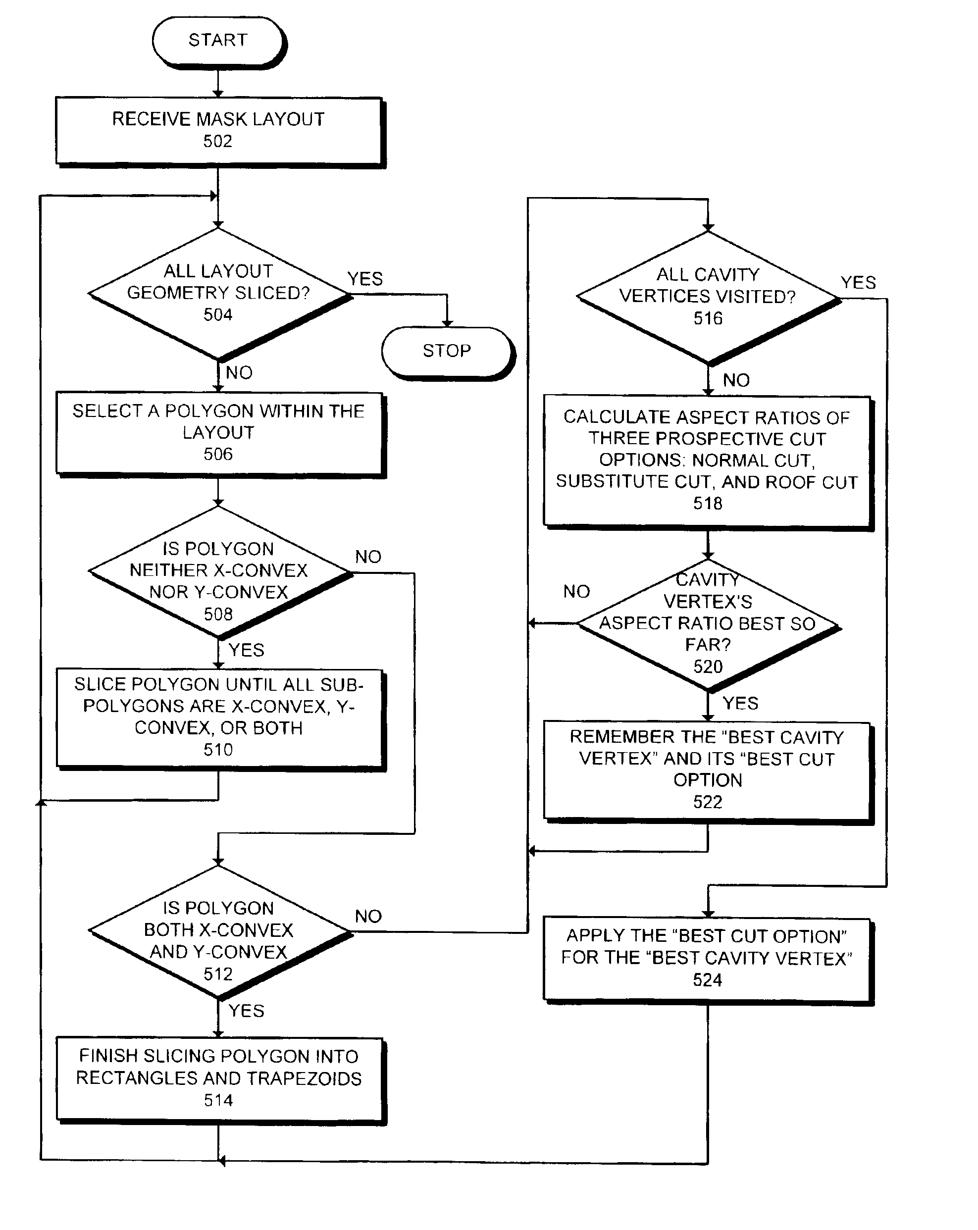
- A method that calculates and selects slices with the smallest aspect ratio for polygons that are either x-convex or y-convex, avoiding extreme aspect ratios and ensuring that all resulting shapes are either rectangles or trapezoids, thereby preventing sliver formation and maintaining consistent critical dimensions.

Super-high aspect ratio diffractive optics fabricated by batch-processing
PatentActiveUS20190154892A1
Innovation
- A method involving a planar substrate with a nanolaminate formed on the sidewall of columns, comprising alternating layers of materials with different refractive indices, supported by a core and surrounded by a frame, allowing for batch processing of diffractive optics with aspect ratios up to tens of thousands to one, using Atomic Layer Deposition (ALD) and conventional semiconductor processing techniques.

Manufacturing Process Integration Considerations
The integration of extreme aspect ratio lithography solutions into manufacturing processes presents multifaceted challenges that extend beyond the lithographic exposure itself. Process integration requires careful orchestration of upstream and downstream manufacturing steps to accommodate the unique requirements of high aspect ratio feature formation while maintaining overall yield and throughput targets.
Substrate preparation becomes increasingly critical when dealing with extreme aspect ratios, as surface planarity and cleanliness directly impact pattern fidelity. Advanced cleaning protocols and chemical mechanical planarization techniques must be optimized to ensure uniform resist coating and minimize defect propagation. The integration timeline must account for extended processing windows, as computational lithography solutions often require longer exposure times and more complex multi-pass sequences.
Resist processing integration demands significant modifications to standard development and post-exposure bake protocols. The thermal budget management becomes crucial, as extreme aspect ratio features are more susceptible to pattern collapse and line edge roughness during processing. Integration teams must establish new process control metrics that specifically monitor aspect ratio uniformity and sidewall quality across the wafer.
Metrology integration poses substantial challenges, requiring deployment of advanced characterization tools capable of measuring high aspect ratio structures. Traditional optical inspection methods prove inadequate, necessitating integration of scanning electron microscopy and atomic force microscopy into routine process monitoring workflows. Real-time feedback systems must be recalibrated to detect aspect ratio-specific defects and process variations.
Equipment integration considerations include modifications to existing lithography tools and potential introduction of specialized hardware for extreme aspect ratio processing. Facility infrastructure may require upgrades to accommodate increased computational requirements for real-time lithography calculations and enhanced environmental controls for improved process stability.
The economic integration model must account for increased cycle times, higher computational overhead, and potential yield learning curves. Manufacturing teams must develop new cost models that balance the premium associated with extreme aspect ratio processing against the value proposition of enhanced device performance and functionality.
Cost-Benefit Analysis of Extreme Aspect Ratio Solutions
The economic evaluation of extreme aspect ratio solutions in computed lithography reveals significant variations in implementation costs across different technological approaches. Traditional optical proximity correction (OPC) methods require substantial computational infrastructure investments, with hardware costs ranging from $500,000 to $2 million for high-performance computing clusters capable of handling complex three-dimensional mask optimization algorithms. The operational expenses include software licensing fees that typically account for 15-25% of annual revenue for mask shops implementing advanced computational lithography solutions.
Source mask blank costs represent another critical economic factor, particularly for extreme ultraviolet (EUV) applications where specialized substrates can cost $50,000-$100,000 per blank compared to $5,000-$15,000 for conventional deep ultraviolet masks. The manufacturing yield rates directly impact the cost-effectiveness, with extreme aspect ratio features showing 10-20% lower yields in initial production phases, translating to increased per-unit costs that must be absorbed during technology maturation periods.
The return on investment analysis demonstrates that companies implementing advanced computational lithography solutions typically achieve break-even points within 18-24 months for high-volume manufacturing scenarios. The primary revenue drivers include reduced mask revision cycles, improved process window margins, and enhanced defect control capabilities. Manufacturing facilities report 30-40% reduction in mask iteration costs when employing sophisticated computational correction algorithms for extreme aspect ratio features.
Comparative analysis between different solution approaches shows that machine learning-enhanced optimization methods require higher initial development investments but offer superior long-term cost efficiency. The total cost of ownership over a five-year period favors hybrid approaches combining traditional rule-based corrections with AI-driven optimization, resulting in 25-35% lower operational costs compared to purely conventional methods.
Risk assessment indicates that delayed implementation of extreme aspect ratio solutions carries significant opportunity costs, particularly as semiconductor nodes advance toward sub-3nm technologies. Early adopters demonstrate competitive advantages through improved time-to-market capabilities and enhanced product performance characteristics, justifying the premium investment requirements associated with cutting-edge computational lithography infrastructure.
Unlock deeper insights with PatSnap Eureka Quick Research — get a full tech report to explore trends and direct your research. Try now!
Generate Your Research Report Instantly with AI Agent
Supercharge your innovation with PatSnap Eureka AI Agent Platform!